Prof. Ohkawa delivers an invited lecture “Micro-LEDs for Display Applications” via Zoom at the Special Symposium on Widegap Semiconductor Optical & Electronic Devices organized by the Japan Society of Wide Gap Semiconductors (WideG).
Prof. Kazuhiro Ohkawa deliver an invited talk at International Workshop on Nitride Semiconductors (IWN). The IWN is a major conference in the fields of LEDs and Lasers. He is the only invited speaker from Saudi Arabia. Mohammed, Artem, and Daisuke give three oral talks and one poster.
Our Scheduled presentation is selected as “Highlighted talk” at the Autumn meeting of the Japanese Society of Applied Physics. Mohammed Najmi et al., “Structural analysis of N-polar InGaN layer grown on ScAlMgO4 substrate without buffer layer” 23a-E202-10 from 11:45 am March 23 (JPN time) The ratio of the highlighted talks in this conference is usually less than 1%.
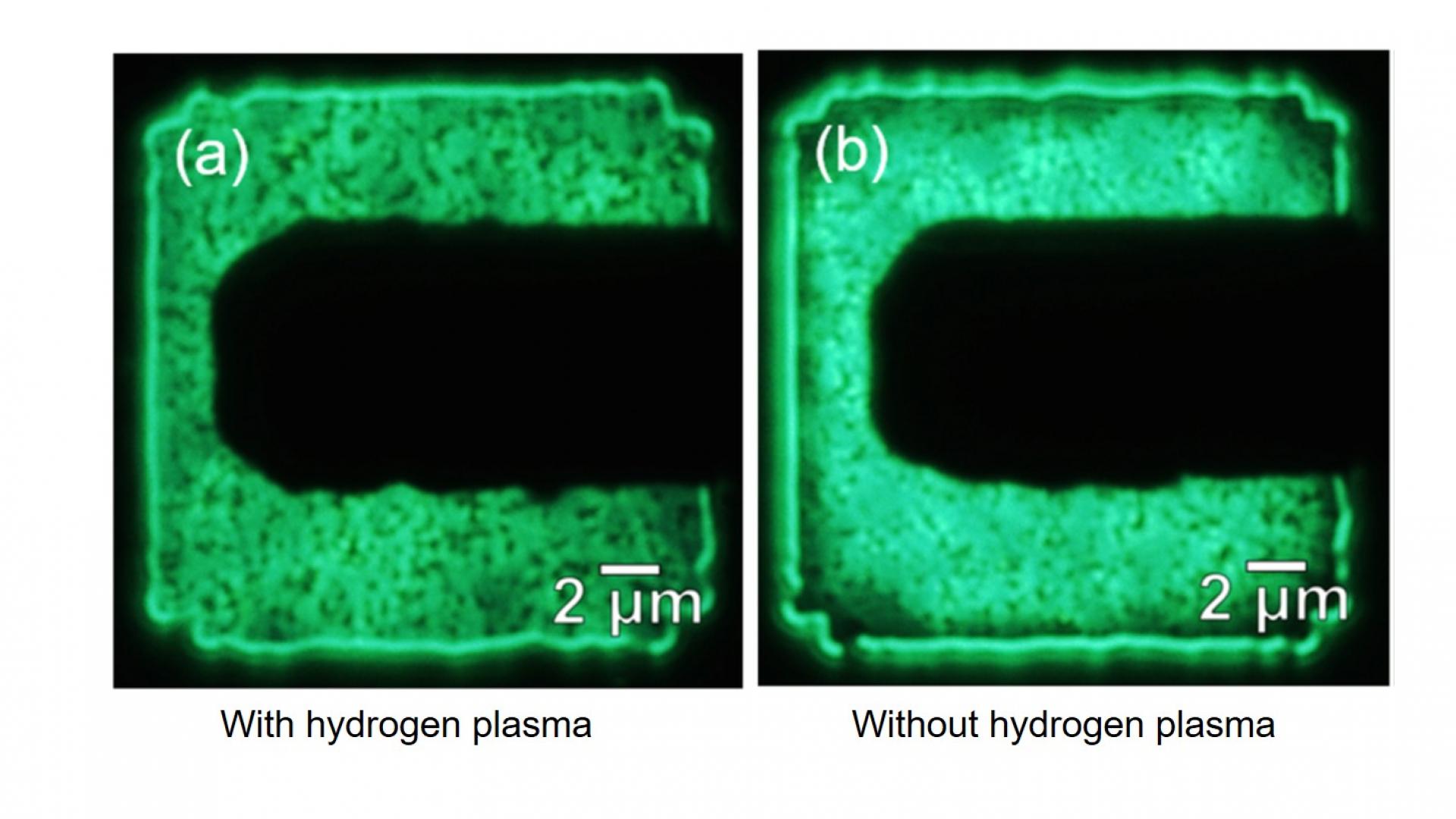
We investigated the effect of the sidewall passivation by hydrogen plasma on the InGaN green micro-LED performance. Hydrogen passivation deactivates the surface region of p-GaN around the perimeter of the device mesa. Thus, hole injection is suppressed in this region, where etchingcaused material degradation results in leakage current, decreasing device efficiency. We have confirmed the hydrogen passivation effect on LED square pixels with sizes of 20 and 100 μm. For smaller LEDs, the reverse leakage current has reduced more than tenfold, and the external quantum efficiency of LEDs was enhanced 1.4-times due to the suppression of the non-radiative recombination.
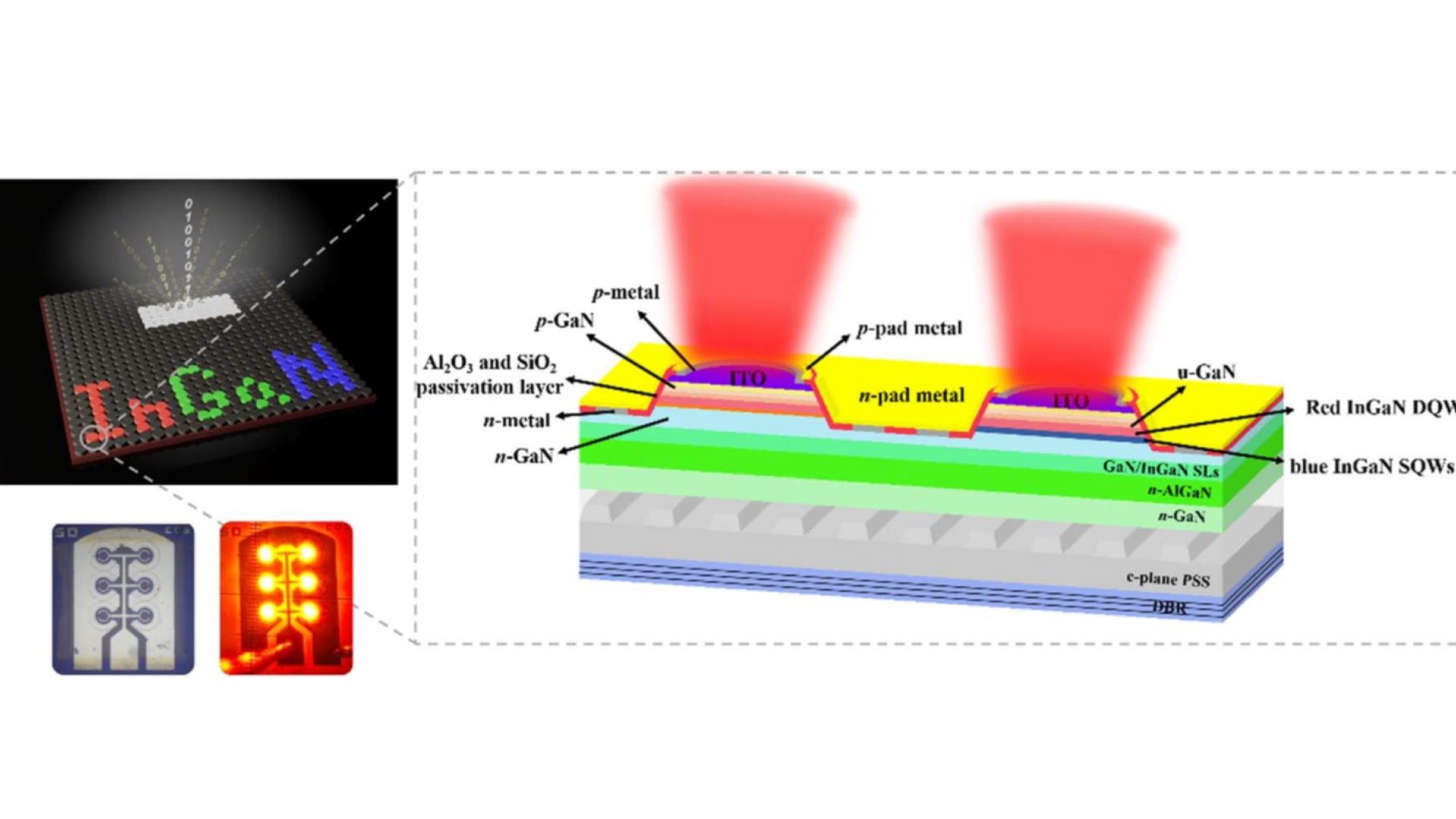
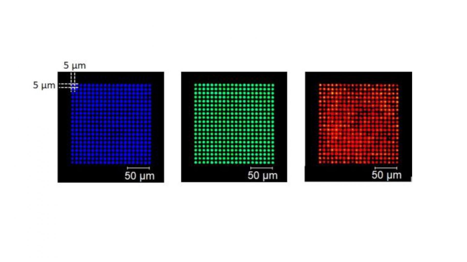
In this study, we present a high-efficiency InGaN red micro-LED fabricated by the incorporation of superlattice
structure, atomic layer deposition passivation, and a distributed Bragg reflector, exhibiting maximum external
quantum efficiency of 5.02% with a low efficiency droop corresponding to an injection current density of
112 A∕cm2. The fast carrier dynamics in the InGaN is characterized by using time-resolved photoluminescence,
which is correlated to a high modulation bandwidth of 271 MHz achieved by a 6× 25-μm-sized micro-LED array
with a data transmission rate of 350 Mbit/s at a high injection current density of 2000 A∕cm2. It holds great
promise for full-color micro-displays as well as high-speed visible light communication applications based on
monolithic InGaN micro-LED technologies.
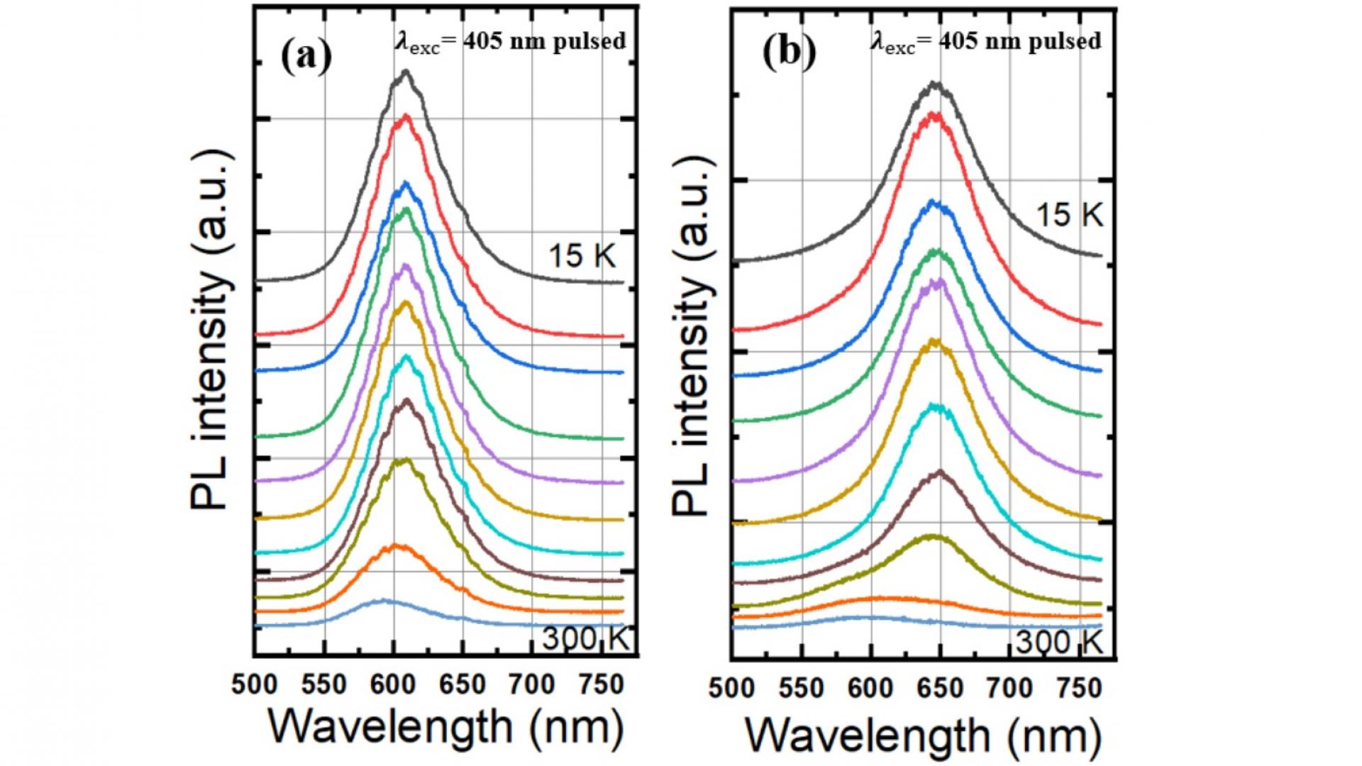
In this work, we present the characterization of red InGaN/GaN multiple-quantum-well (MQW) light-emitting diode (LED) structures. The results of photoluminescence (PL) studies show that a thicker n-GaN layer is beneficial for obtaining higher In-content for red MQWs. Our findings imply that in order to achieve high-efficiency InGaN MQWs for red emission, enhancing the uniformity of In-content distribution in the active region and decreasing non-radiative recombination centers are critical challenges.
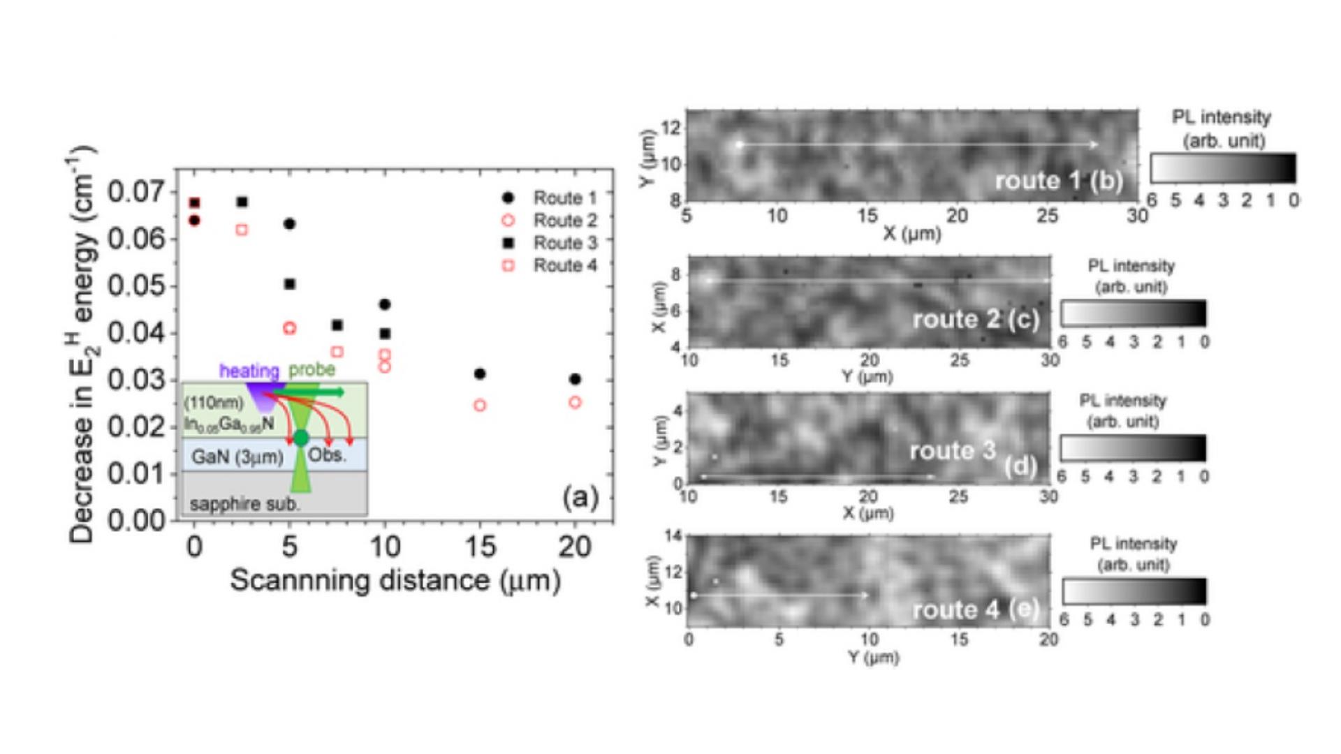
The pump and probe technique in Raman spectroscopy is used to demonstrate the phonon transport properties of an In0.05Ga0.95N/GaN heterostructure. This method has the advantage of enabling the study of phonon transport processes inside and at interfaces of films with crystal defects by visualizing the shift of phonon-mode energies due to local heating.
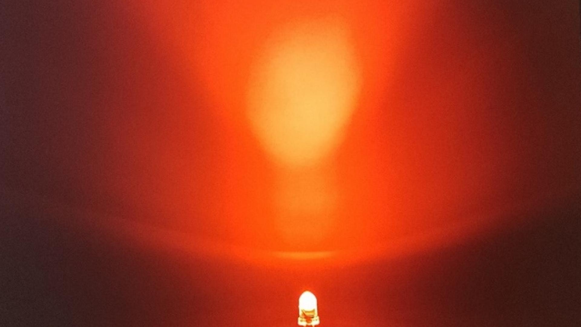
We report highly efficient InGaN-based red light-emitting diodes (LEDs) grown on conventional c-plane-patterned sapphire substrates. The packaged LED's external quantum efficiency, light-output power, and forward voltage with a 621 nm peak emission wavelength at 20 mA (10.1 A/cm2) injection current were 4.3%, 1.7 mW, and 2.96 V, respectively. This design development represents a valuable contribution to the next generation of micro-LED displays. This paper has been chosen as an Editor's Pick.
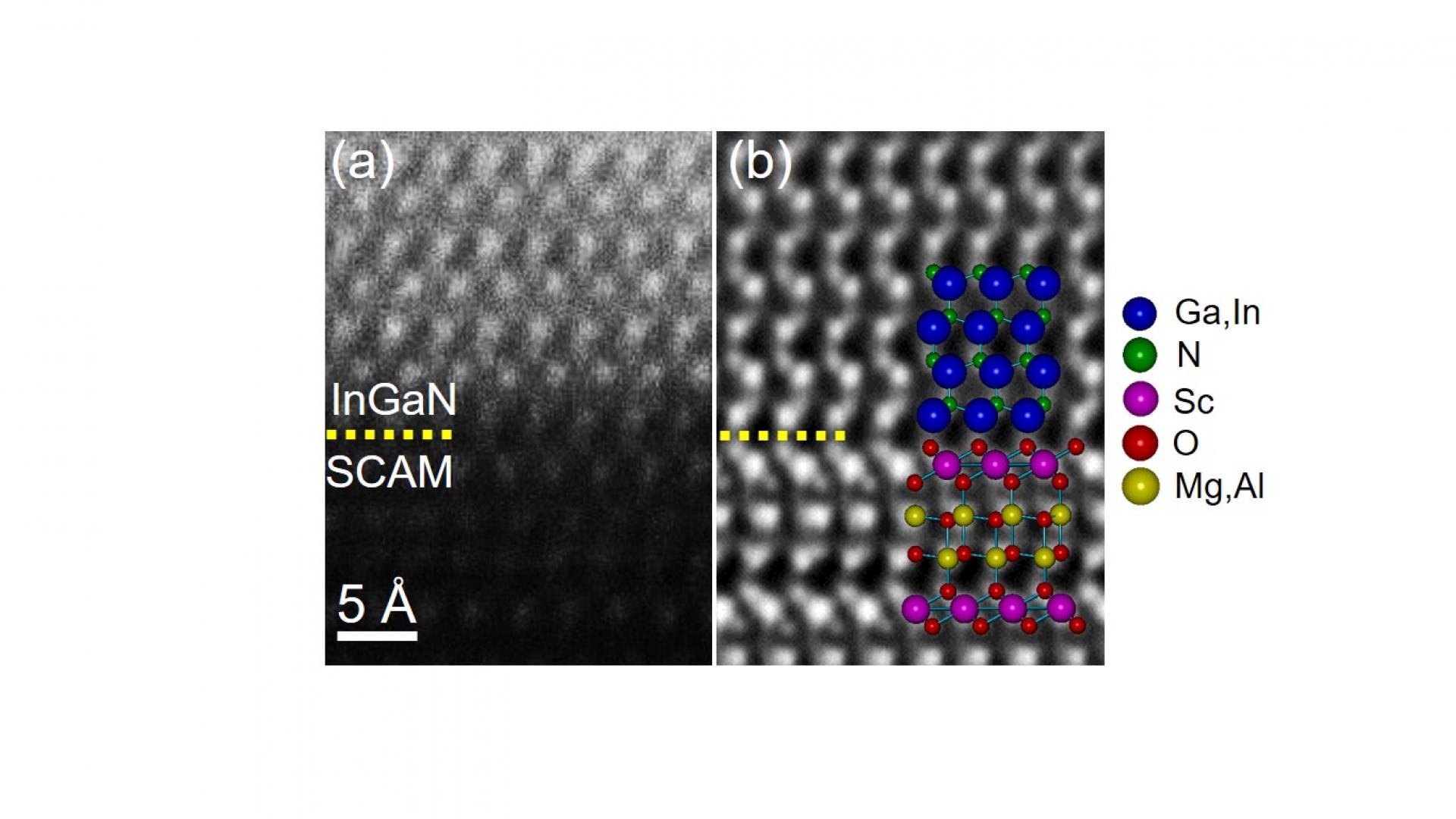
We demonstrated a high crystalline quality of N-polar InGaN layer grown on ScAlMgO4 substrates by metalorganic vapor-phase epitaxy. The results show that the interface between N-polar InGaN and SAM occurs between the O atoms of the O–Sc SAM surface and the (Ga,In) atoms of InGaN.

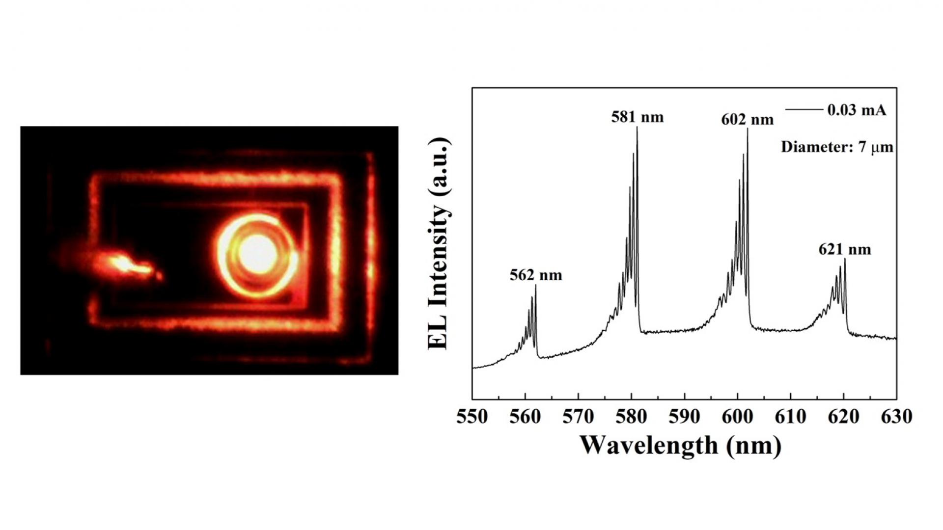
We demonstrated that the InGaN-based red resonant cavity LEDs exhibited optical resonant effect, a high Q factor (~3010), and a narrow emission linewidth (FMHW ~0.2 nm), indicating low optical loss in the resonant cavity.
Our Scheduled presentation is selected as “Highlighted talk” at the Spring meeting of the Japanese Society of Applied Physics in Spring 2022.
Daisuke Iida et al., “” 23a-E202-10 from 11:45 am March 23 (JPN time)
The ratio of the highlighted talks in this conference is usually less than 1%.

Prof. Kazuhiro is appointed a Guest Professor at Xiamen University (China) from February 2022.

Prof. Kazuhiro is appointed a Visiting Professor at Mie University (Japan) from November 2021.
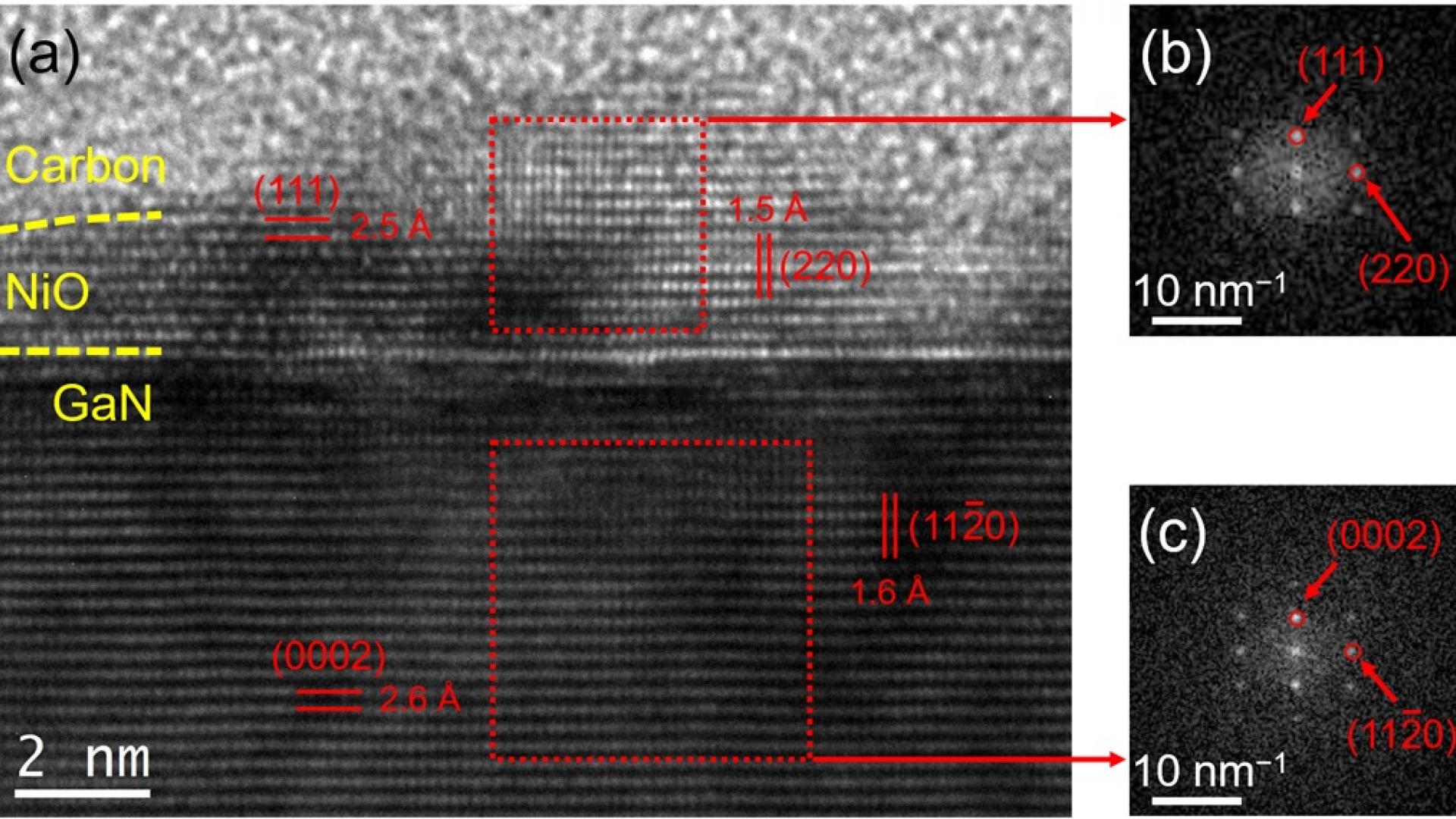
we characterized the surface states in GaN by EIS analyses and demonstrated that NiO particles deposited directly on GaN passivate them. These surface states are generated by the electronic bindings of superficial Ga atoms, and the interaction of those atoms with NiO modifies its chemical structure, as demonstrated by XPS measurements.