Metamaterials consist of engineered periodic or aperiodic composites that collectively behave as an effective, innovative material. They exhibit peculiar properties that are mostly not observed naturally. They offer significant potential for numerous applications due to their uniqueness, and there is an increasing interest in developing innovative materials to offer novel functionalities. Our energetic team at ITL is working enthusiastically to design and develop innovative artificially-engineered materials for a broad range of promising areas like renewable energy harvesting, autonomous diagnostics solutions for healthcare, next-generation holographic displays, and bio-sensing. Meanwhile, the team also focuses on developing soft-solutions for artificially-engineered materials, such as intelligent optimization tools for efficiently designing nano-devices and algorithms' development for an autonomous decision-support platform. A brief description of a few highlighted themes is provided below.
Intelligent Nanophotonics
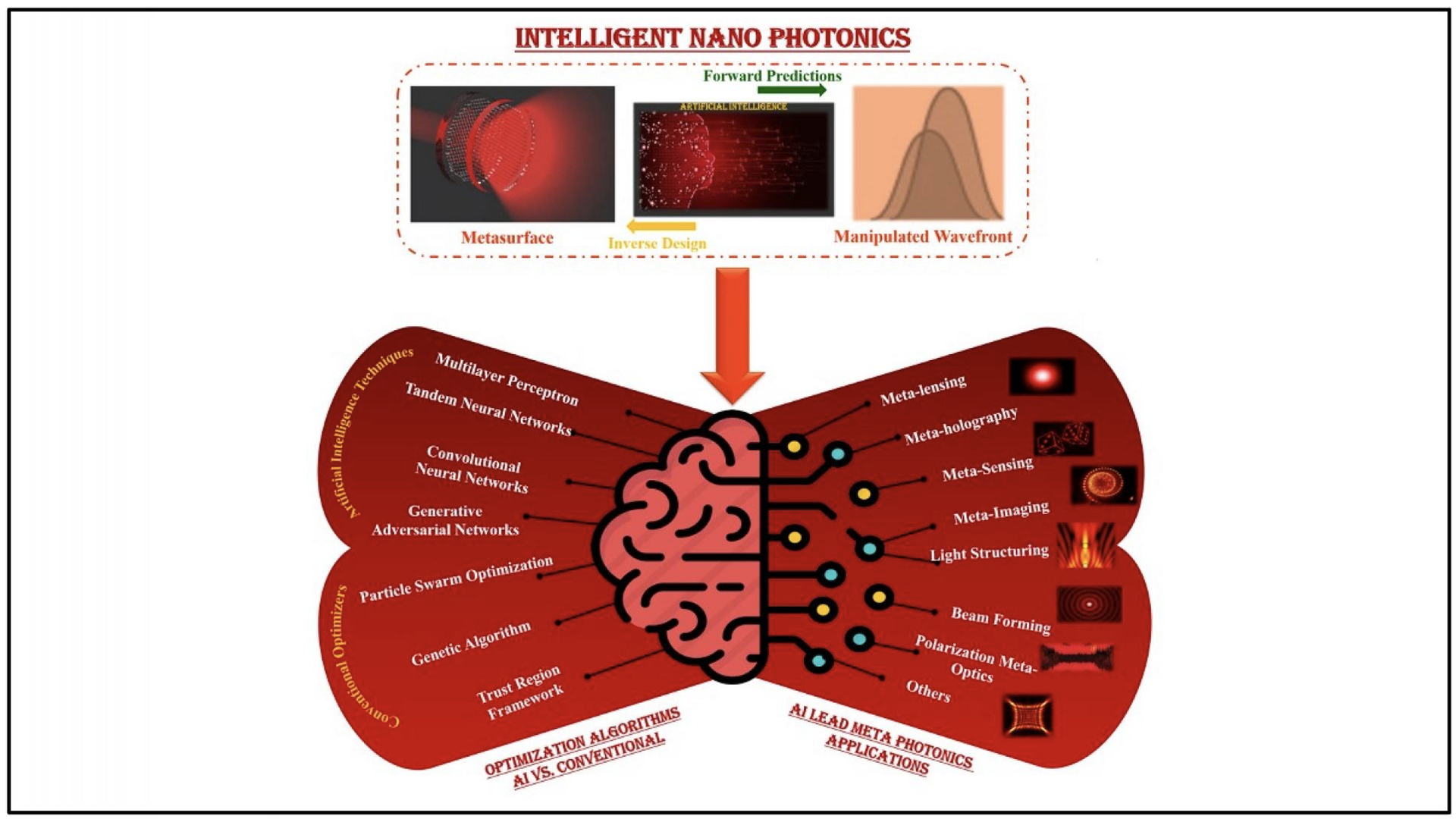
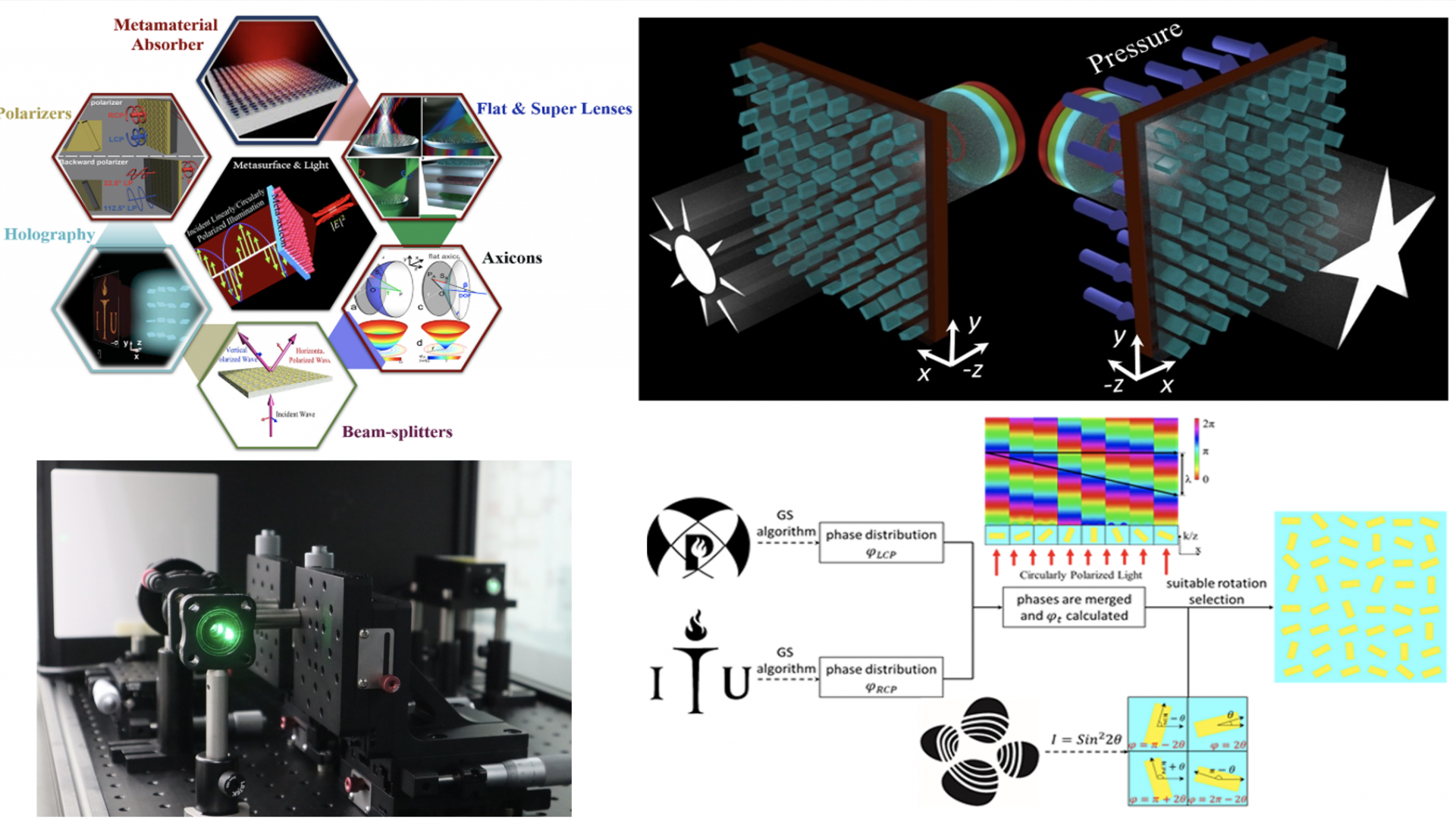
Modern-day science and technology have used metamaterials and metasurfaces over the entire electromagnetic spectrum. When these applications are light-based, the particular niche assumes the name “metaphotonics”. The associated devices – “metadevices” – feature miniaturized fabrication to achieve planar, ultrathin, multifunctional electromagnetic systems. Metasurfaces are branded as next-generation lightweight and fabrication-friendly optical components. They are found in high-capacity data transmission, super-resolution imaging employing metamicroscopy and enabling automated diagnostics solutions, metaholograms for holographic displays, metadevices-assisted efficient solar energy harvesting, meta-surfaces for advanced biosensing and bioimaging, and reconfigurable intelligent surfaces for wireless networks. The field of meta-photonics now benefits from 2D materials-based meta-surface design techniques that have succeeded in further reducing device footprints for better integration in optoelectronic devices. Furthermore, intelligent metaphotonics is gaining popularity, and machine learning-assisted global optimization is being explored for metasurfaces.

Our energetic team at ITL is working enthusiastically to develop various multifunctional metaphotonics platforms and metadevices for next-generation holographic displays, advanced biosensing, smart metamicroscopy, solar energy harvesting, and next-generation wireless communications. Our research aims to develop advanced neural networks capable of predicting the electromagnetic response within a fraction of seconds, thus replacing the time-consuming conventional iterative process EM solvers. In addition, we are also working to develop inverse design models to optimize the structural parameters and shape of a metasurface to achieve the desired optical response.
Next-generation Holographic Displays
Holography is an ideal method to generate three-dimensional displays of great originality and vividness, visible to the naked eye. Industrial applications of holograms include information encryption, 3D security tags, and anti-counterfeiting images on credit cards and banknotes. Many traditional holograms are unable to portray images. As nanofabrication technology progresses, the meta-holograms are becoming striking hotspots for next-generation holographic displays. Meta-holograms replace the conventional bulky elements and provide superior functionalities with miniaturized footprints. Compared to conventional photography, with the extraordinary capability of storing intensity and phase information of any image, meta-holograms can capture a great amount of information about a picture. Meta-holography-based optical elements are suitable for product integration by thermoforming, lamination, plastic injection molding, and casting.

Customized Smart Bio-imaging & Sensing

Bio-imaging and sensing are of great significance for the early detection, rapid diagnosis, and precise treatment of diseases. They effectively expand human eyesight to micro and nano-scales. Emergent demand in biological research for super-resolution, extraordinary throughput, and imaging capacity leads to ever more complex and expensive microscopes. Their optical setups are getting immensely complex due to bulky optical components to improve the performance. Situations become more crucial with hardware specificity which restricts to modify or even reconfigure optical systems, which leads to the high demand for handcrafted adapters or unnecessarily long attachments compromising the system’s integrity and stability. Moreover, Refractive elements enabled traditional imaging systems unable to achieve the ultimate goal of ultra-compactness, miniaturized devices with comprehensive performance for wide field-of-view (FOV), large depth-of-field (DOF), and high throughput. What we see as a generous space for improvement, is straightforward interfacing between constituents of modern imaging systems comprising sources, metasurface-enabled optics, and detector components. Such a platform would expedite simple assemblies of versatile imaging instruments, a high degree of customization to almost any imaging solution. Metalens technology unties a new tactic to realize ultra-compact and lightweight optical imaging systems. A metalens is a kind of metasurface composed of subwavelength resonating antennas with powerful capability for manipulating light and thus, able to significantly improve imaging quality with higher-resolution, wide FOV and DOF.
Reconfigurable Intelligent Surfaces for Wireless Networks

Reconfigurable Intelligent Surfaces (RIS) are a class of metasurfaces that contain switching elements that allow the electromagnetic (EM) response of RIS to be dynamically controlled. RIS can be employed as modulators and relays by transmitting EM waves through or reflecting off of RIS. RIS can be utilized to enhance quality of service (QoS) by bypassing blockage and assisting wireless communication through virtual line of sight paths. Next generation wireless networks (6G) will be able to take advantage of non-obtrusive RIS deployed on walls and windows of Smart Cities. RIS can make the wireless channel a controllable variable and allow 6G to achieve Tb/s data transfer rates with sub-millisecond latency and very low probability of outage.
Smart cities will incorporate RIS in the infrastructure. RIS as an integral part of “living surfaces” will allow and IoT-enabled bio-nano sensors and passive metadevices embedded in the furniture to take advantage of ubiquitous connectivity. We at ITL KAUST are focusing on various directions in this regard such as
- Algorithms for RIS design and optimization
- RIS fabrication and deployment
- RIS characterization and standardization
- Large scale low power RIS implementation challenges for Smart Cities
- RIS based physical layer strategies for wireless communication