Metamaterials consist of engineered periodic or aperiodic composites that collectively behave as an effective, innovative material. They exhibit peculiar properties that are mostly not observed naturally. They offer significant potential for numerous applications due to their uniqueness, and there is an increasing interest in developing innovative materials to offer novel functionalities. Our energetic team at ITL is working enthusiastically to design and develop innovative artificially-engineered materials for a broad range of promising areas like renewable energy harvesting, autonomous diagnostics solutions for healthcare, next-generation holographic displays, and bio-sensing. Meanwhile, the team also focuses on developing soft-solutions for artificially-engineered materials, such as intelligent optimization tools for efficiently designing nano-devices and algorithms' development for an autonomous decision-support platform. A brief description of a few highlighted themes is provided below.
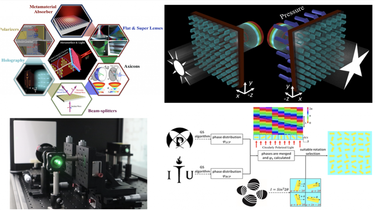
Intelligent Nanophotonics
Modern-day science and technology have used metamaterials and metasurfaces over the entire electromagnetic spectrum. When these applications are light-based, the particular niche assumes the name “metaphotonics”. The associated devices – “metadevices” – feature miniaturized fabrication to achieve planar, ultrathin, multifunctional electromagnetic systems. Metasurfaces are branded as next-generation lightweight and fabrication-friendly optical components. They are found in high-capacity data transmission, super-resolution imaging employing metamicroscopy and enabling automated diagnostics solutions, metaholograms for holographic displays, metadevices-assisted efficient solar energy harvesting, meta-surfaces for advanced biosensing and bioimaging, and reconfigurable intelligent surfaces for wireless networks. The field of meta-photonics now benefits from 2D materials-based meta-surface design techniques that have succeeded in further reducing device footprints for better integration in optoelectronic devices. Furthermore, intelligent metaphotonics is gaining popularity, and machine learning-assisted global optimization is being explored for metasurfaces.
Our energetic team at ITL is working enthusiastically to develop various multifunctional metaphotonics platforms and metadevices for next-generation holographic displays, advanced biosensing, smart metamicroscopy, solar energy harvesting, and next-generation wireless communications. Our research aims to develop advanced neural networks capable of predicting the electromagnetic response within a fraction of seconds, thus replacing the time-consuming conventional iterative process EM solvers. In addition, we are also working to develop inverse design models to optimize the structural parameters and shape of a metasurface to achieve the desired optical response.
Spintronic Materials and Devices
Conventional electronic devices are based on nonmagnetic semiconductors and use the controlled flow of electric charges to achieve information processing and communication. Spintronic devices, on the other hand, exploit the spin of electrons to generate and control charge currents, and to interconvert electrical and magnetic signals. By combining processing, storage, sensing, and logic within a single integrated platform, spintronics could complement and, in some cases, outperform semiconductor-based electronics, offering advantages in terms of scaling, power consumption, and data processing speed. Spintronics has the potential to play a major role in the future of the microelectronics industry and biotechnology area.
The ability to electrically control the magnetization in spintronics devices along with low operational voltage, non-volatility, adaptive and fault tolerant ability, integration with CMOS based devices, makes them a potential candidate for future computing paradigms like Neuromorphic computing, probabilistic computing, Combinatorial optimization, Bayesian Inference, Next generation memory devices, Reversible logic, Ising Computation etc. The idea of utilizing the spin for information encoding in the form of up-spin and down-spin is paving the way for Innovative technologies for information processing and transmission. The KAUST ITL team focus spans a wide range of spintronics-related fields including magnetic materials, spintronics theory, spin-based devices, circuits utilizing the spin, novel architecture and algorithms, understanding the computing principle and finally the fabrication of such devices.
Hardware Security
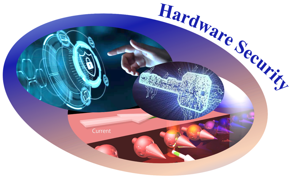
The increasing threat of security attacks on hardware security applications has driven research towards exploring beyond CMOS devices as an alternative. Spintronic devices offer certain advantages like low power, non-volatility, inherent spatial and temporal randomness, simplicity of integration with silicon substrate etc. making them a potential candidate for next generation hardware security systems. In this work, we explore several emerging structures based on MTJ for possible logic locking applications. The integrated circuits (ICs) are commonly recognized as a source of trust in the Internet-of-Things (IoT) applications. However, globalization of integrated circuit (IC) design and fabrication has led to growing cost and design complexity that resulted in severe security concerns. As a result, the majority of the IC design companies have gone fabless due to their heavily relying on untrusted foundries to fabricate their ICs. In the semiconductor sector, insertion of hardware Trojans, reverse engineering attacks, side channel attacks, piracy of intellectual property (IP), counterfeiting of chips, overbuilding and other have raised both hardware security threats and financial losses. The emergence of spintronics devices and their easy integration with Si substrate has made them a potential candidate for both Attack and Defense mechanism. The ITL group will focus on developing new possible Attack algorithms and proper counter mechanisms to ensure that the security of hardware systems remain intact. Spintronics based devices have shown potential for non-Boolean computation to fight the Von-Neumann bottleneck like Neuromorphic computing, Non-volatile memory, In-memory computing etc. With advancement in Fabrication technology, more hardware systems based on Hybrid spintronics, and CMOS structure will be available for commercial use.
Spintronics Platforms for Biomedical Applications

Advances in the Tunneling MagnetoResistive (TMR) sensors technology (higher sensitivity, smaller size) have potentiated biomedical applications, plants and Agriculture studies. The investigation of spintronics and its applications to the development of magnetoresistive (MR) biomolecular and biomedical platforms are giving rise to a new class of biomedical diagnostic devices, suitable for bench top bioassays as well as point-of-care and point-of-use devices. Lab-on-a-chip MR-based platforms to perform biological studies at the single molecule level are one of main targets in our group.
Spintronics in two-dimensional materials
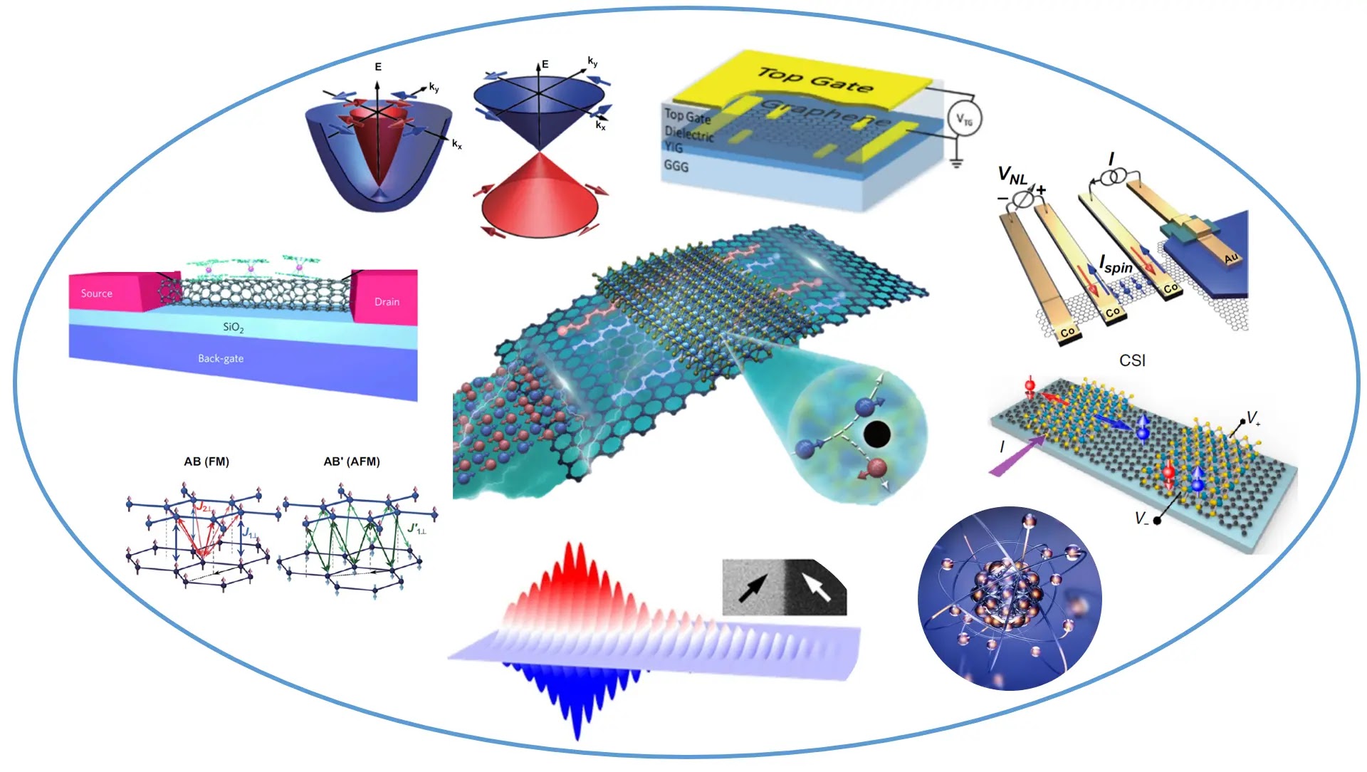
Recently, two-dimensional (2D) materials have gain significant attention in spintronics owing to their unique spin-dependent properties, such as the ultra-long spin relaxation time of graphene and the spin–valley locking of transition metal dichalcogenides. Moreover, the additional advantage of making heterostructures provide an unmatched probability of combining the different characteristics via proximity effect, which could not only rectify the shortcomings of individual 2D materials but can also open new avenues to explore as well. Here in ITL, we explore the physics behind spin injection, transport, manipulation, and application for information storage and processing.