© 2017 KAUST
The electronic characteristics of an interface between two wide bandgap semiconductors are determined by researchers at KAUST: an insight that will help improve the efficiency of light-emitting and high-power electronic devices.
Semiconductors, such as silicon and gallium nitride, have electrical properties somewhere in between those of a conductor and an insulator. They only allow current to flow when electrons have enough energy to overcome a barrier known as bandgap. The bandgap—which may be direct or indirect, narrow or large—determines the properties of semiconductors and their consequent applications.
Materials with a large bandgap, for example, are useful in high-power electronics because they have larger breakdown voltage for energy-efficient transistors as compared with narrow bandgap materials, such as silicon. They can also produce light deep into the ultraviolet part of the spectrum, making them useful for disinfection and water purification.
These materials can be further tailored to a specific application by layering different semiconductors on top of each other to create a so-called heterostructure with the desired properties. But it is vital to understand how the bandgaps of two semiconductors align when semiconductors are brought together in this way.
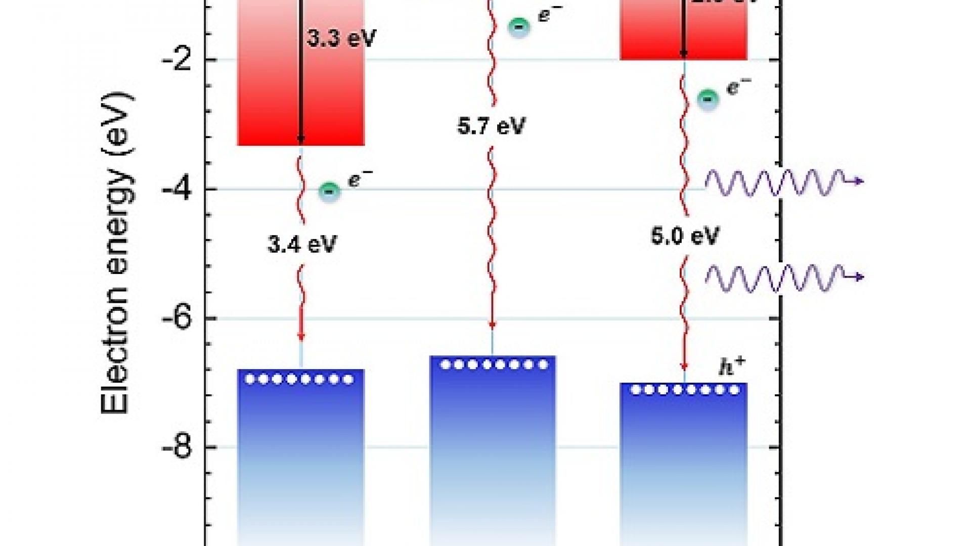
Haiding Sun and principle investigator Xiaohang Li from KAUST and coworkers from the Georgia Institute of Technology, USA, report that they experimentally measured the alignment of two emerging large bandgap materials: boron aluminum nitride and aluminum gallium nitride.
Read the full article
Related Persons