Nanoscale patterning is better with gas
Adding a gas enhances the processing of hybrid organic-inorganic materials for improved solar cells.
About
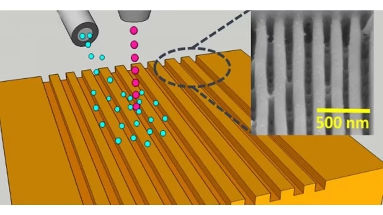
A technique developed by KAUST scientists has made more controlled fabrication of optoelectronic devices produced from a hybrid of organic and inorganic materials possible.
Solar cells that are based on a perovskite material made by combining organic methylammonium ions with inorganic lead atoms plus a halide (chlorine, bromine or iodine) atom have already shown high efficiency and are economical to produce.
A drawback, however, is that the organic component is sensitive to the solvents and temperature changes that are often involved in device fabrication.
“Perovskite is a relatively new material, so fabrication technology is not well-developed,” said KAUST Professor of Electrical Engineering Boon Ooi. “Existing approaches are at the microscale and inhomogeneous.”
Ooi and his colleagues from the University's Photonics Laboratory, the Imaging & Characterization Core Lab and the Solar & Photovoltaics Engineering Research Center have demonstrated a technique that can directly pattern perovskites with features smaller than one micrometer with little surface damage.
Read the full article
