Advanced ultrawide bandgap semiconductors for ultraviolet photonics
The advancement of silicon semiconductor technology since the 1940s has been changing the world by redefining human living style and addressing global challenge of energy shortage. Since the 1960s, GaAs, InP research started to bring human beings into modern life with mobile communications and high-speed networks. When it goes to the 1980s, wide band gap semiconductors including GaN and SiC which have high breakdown field and high mobility, were demonstrated into high-power electronics as well as solid-state lighting.
Overview
Abstract
The advancement of silicon semiconductor technology since the 1940s has been changing the world by redefining human living style and addressing global challenge of energy shortage. Since the 1960s, GaAs, InP research started to bring human beings into modern life with mobile communications and high-speed networks. When it goes to the 1980s, wide band gap semiconductors including GaN and SiC which have high breakdown field and high mobility, were demonstrated into high-power electronics as well as solid-state lighting. All the three waves have built the modern society today. Lately, ultrawide bandgap (UWBG) semiconductors with bandgap larger than 3.4 eV, including III-Nitride, and III-Oxide, have emerging as the next generation semiconductor, allowing for the greater power electronics and UV photonics. However, numerous investigations of material growth, physics, and device fabrication are critical to reveal their application potentials. In this talk, we will introduce the latest research on ultraviolet photonic devices based on III-Nitride and III-Oxide UWBG semiconductors. It covers the design and growth of efficient III-Nitride UV LEDs for radiative sterilization (e.g. Covid-19 virus) by employing polarization engineering. Moreover, ultra-sensitive UV photodetector driven by III-Oxide thin film membrane will be included for advance imaging and sensor system. Lastly, we would show the investigation of III-Nitride/III-Oxide heterogeneous integration for emerging device physics and material science.
Brief Biography
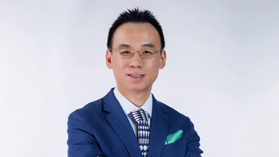
Yi Lu is a Ph.D candidate in the Advance Semiconductor Lab in KAUST since Aug. 2019. He obtained his master degree from Institute of Semiconductors, Chinese Academy of Sciences in 2019, and bachelor degree from Taiyuan University of Technology in 2016. His research focuses on modeling, epitaxy, and fabrication of III-Nitride and III-Oxide based optoelectronic devices. He is the recipient of the 1st place scientific talks in KAUST Research Open Week 2021 and best poster award in Future of Semiconductors Forum 2022. He is also the student ambassador in CEMSE division since July 2021.
