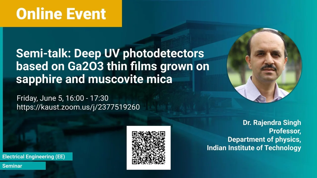
Semi-talk: Deep UV photodetectors based on Ga2O3 thin films grown on sapphire and muscovite mica
- Prof. Rajendra Singh, Indian Institute of Technology Delhi
KAUST
Dr. Rajendra Singh is presently a Professor at the Department of Physics, IIT Delhi. He did M.Sc. (Physics) from D.B.S. College, Dehra Dun (affiliated to H.N.B. Garhwal University) in 1995. After that he joined Inter University Accelerator Centre (formerly Nuclear Science Centre), New Delhi for Ph.D. His Ph.D. work was related to the study of the effect of swift heavy ion irradiation on electrical properties of Si and GaAs. He completed his Ph.D. in 2001 with degree from Jawaharlal Nehru University, New Delhi. He then joined Walter Schottky Institute (WSI), Technical University of Munich (TUM), Germany as a post doctoral fellow. There he worked on the design, fabrication and characterization of InP-based heterojunction bipolar transistors (HBTs). He extensively used Class 100 Cleanroom facilities at WSI working on various processing tools such as photolithography, wet etching, reactive ion etching, UHV metallization and rapid thermal annealing. In January 2004 he joined the Max Planck Institute of Microstructure Physics, Halle, Germany as a post doctoral fellow. There he worked in the area of direct wafer bonding and layer splitting of semiconductors for the fabrication of silicon-on-insulator (SOI) and strained silicon-on-insulator (sSOI). He worked in a Class 10 Cleanroom facility at MPI Halle using processing tools such as wet benches, wafer bonding system, plasma enhanced chemical vapour deposition (PECVD) and annealing furnaces.
Overview
Brief Biography
Dr. Rajendra Singh is presently a Professor at the Department of Physics, IIT Delhi. He did M.Sc. (Physics) from D.B.S. College, Dehra Dun (affiliated to H.N.B. Garhwal University) in 1995. After that he joined Inter University Accelerator Centre (formerly Nuclear Science Centre), New Delhi for Ph.D. His Ph.D. work was related to the study of the effect of swift heavy ion irradiation on electrical properties of Si and GaAs. He completed his Ph.D. in 2001 with degree from Jawaharlal Nehru University, New Delhi. He then joined Walter Schottky Institute (WSI), Technical University of Munich (TUM), Germany as a post doctoral fellow. There he worked on the design, fabrication and characterization of InP-based heterojunction bipolar transistors (HBTs). He extensively used Class 100 Cleanroom facilities at WSI working on various processing tools such as photolithography, wet etching, reactive ion etching, UHV metallization and rapid thermal annealing. In January 2004 he joined the Max Planck Institute of Microstructure Physics, Halle, Germany as a post doctoral fellow. There he worked in the area of direct wafer bonding and layer splitting of semiconductors for the fabrication of silicon-on-insulator (SOI) and strained silicon-on-insulator (sSOI). He worked in a Class 10 Cleanroom facility at MPI Halle using processing tools such as wet benches, wafer bonding system, plasma enhanced chemical vapour deposition (PECVD) and annealing furnaces. There he also initiated activities on hydrogen implantation induced layer splitting (called as ion cut process) of GaN, AlN and ZnO. He joined the Department of Physics, IIT Delhi in November, 2006. His areas of interest are GaN based materials and devices, growth and characterization of semiconductor nanowires, wafer bonding and layer splitting of crystalline materials, graphene-semiconductor interfaces, and 2D materials and devices.
