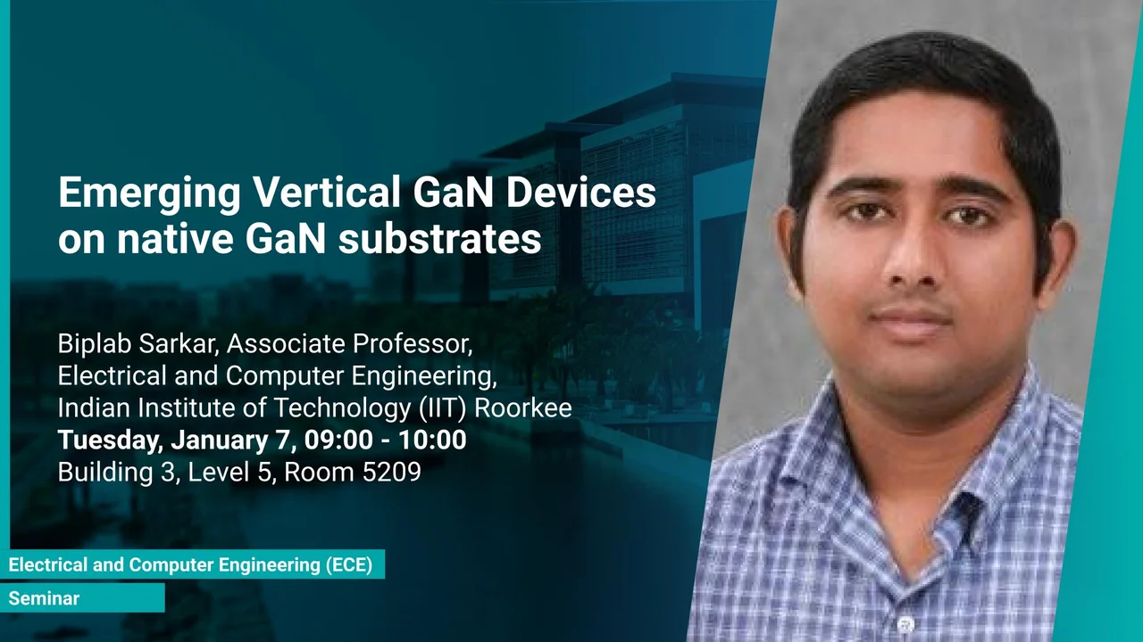
Emerging Vertical GaN Devices on native GaN substrates
This talk will explore emerging vertical GaN devices on native substrates, including (i) GaN JBS diode, (ii) vertical junctionless GaN Fin-MOSFETs, (iii) vertical GaN (trench) MOSFETs, etc., to address limitations of lateral GaN HEMTs at high voltages, while also discussing device and process challenges and concluding with an examination of Fermi-level pinning effects on the GaN surface.
Overview
Lateral GaN HEMTs are already enjoying rapid market adoption. However, scaling of lateral GaN HEMTs to higher voltages demands a higher footprint as well as compromised ON-resistance. To counter these issues, vertical GaN devices on native GaN substrates are attracting global attention. Several emerging GaN devices on GaN substrates are currently under development, such as (i) GaN JBS diode, (ii) vertical junctionless GaN Fin-MOSFETs, (iii) vertical GaN (trench) MOSFETs, etc. In this talk, we will discuss these devices and their unique proprieties apart from understanding the device-related and process-related challenges. The talk will conclude with my recent understanding of the GaN surface – particularly on understanding the fermi-level pinning effect.
Presenters
Biplab Sarkar, Associate Professors, Electrical and Computer Engineering, Indian Institute of Technology (IIT) Roorkee
Brief Biography
Dr. Biplab Sarkar is an Associate Professor at the Indian Institute of Technology (IIT) Roorkee. He is currently involved in the development of commercial-grade (ultra)wide bandgap semiconductor based electronic devices. He completed his PhD from NC State University, the USA in 2015 where he worked on semiconductor memory devices. Later on, he also did postdoctoral research at NC State University in the area of wide & ultrawide bandgap semiconductor devices. His research expertise encompasses device processing, electrical-&-physical characterization, and device modeling. He has demonstrated bulk epitaxial growth methods to achieve high crystalline quality GaN and AlGaN films. Apart from nitride semiconductors, he has also demonstrated near-ideal and homogeneous Schottky diodes using β-Ga2O3 films grown using the Czochralski method. Over the past few years, he has demonstrated high brightness LEDs, self-powered photodiodes, high voltage Schottky diodes, and AlGaN/GaN HEMTs for RF applications. He has served as a committee member of the 2020 UV light emitters roadmap. He was invited to be a panelist in the power electronic device segment of the VAIBHAV Summit 2020 organized by the Prime Minister’s Office, Govt. of India. He is a recipient of the prestigious JSPS Fellowship, 2022. He has published more than 50 journal articles and holds visiting faculty status at the NC State University.