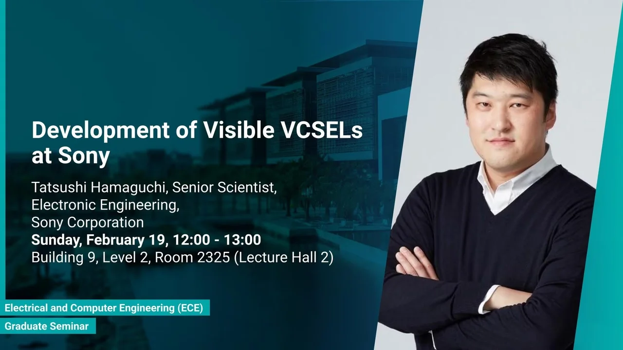
Development of Visible VCSELs at Sony
- Tatsushi Hamaguchi, Electronic Engineering, Sony Corporation
B9 L2 H2
Visible VCSELs have been attracting researchers' interest for potential applications as light sources for optical storage, laser printers, projectors, displays, solid-state lighting, optical communications, biosensors, and so on.
Overview
Abstract
Visible VCSELs have been attracting researchers’ interest for potential applications as light sources for optical storage, laser printers, projectors, displays, solid-state lighting, optical communications, biosensors, and so on. The small power consumption of VCSELs is expected to enable ultra-small, energy-efficient wearable displays, and the expectation drives companies to develop this kind of lasers. This lecture introduces the latest progress of Sony’s visible VCSELs, especially blue and green ones made of GaN-based materials.
Brief Biography
Tatsushi HAMAGUCHI was born in Osaka, Japan in 1980. He received his B.S. and M.S. degrees in material science and engineering from Kyoto University in 2004 and 2006. He received a Ph.D. degree in electronic engineering from Sophia University in 2019. From 2006 to 2008, he worked at the Nitride Semiconductor Research Laboratory of Nichia Corporation. After 2008, he worked for Sony Corporation, where he did the development of nitride-based edge-emitting lasers and vertical-cavity surface-emitting lasers (VCSELs). He has acted as a senior scientist to lead Sonyʼs project team for nitride-based VCSELs in recent years. He received Sony Outstanding Engineer Award in 2019 and JSAP Outstanding Paper Award in 2021.
