Details
The semiconductor industry is facing a technological crisis, as the power density of integrated circuit “chips” has been constantly increasing for CMOS technology nodes below 90 nm, a consequence of increasing transistor OFF-state leakage current with miniaturization. The aim of this project is to address this problem by incorporating compact, zero-leakage switching devices as additional building blocks for integrated circuits, to enhance the energy efficiency and functionality of future integrated systems.
Although microelectromechanical (MEM) relays have been introduced as an appealing class of such alternative switches, their large footprints, slow operation, large operational voltage, and lack of analog functionality have undermined their near ideal switching behavior (zero OFF-state leakage).
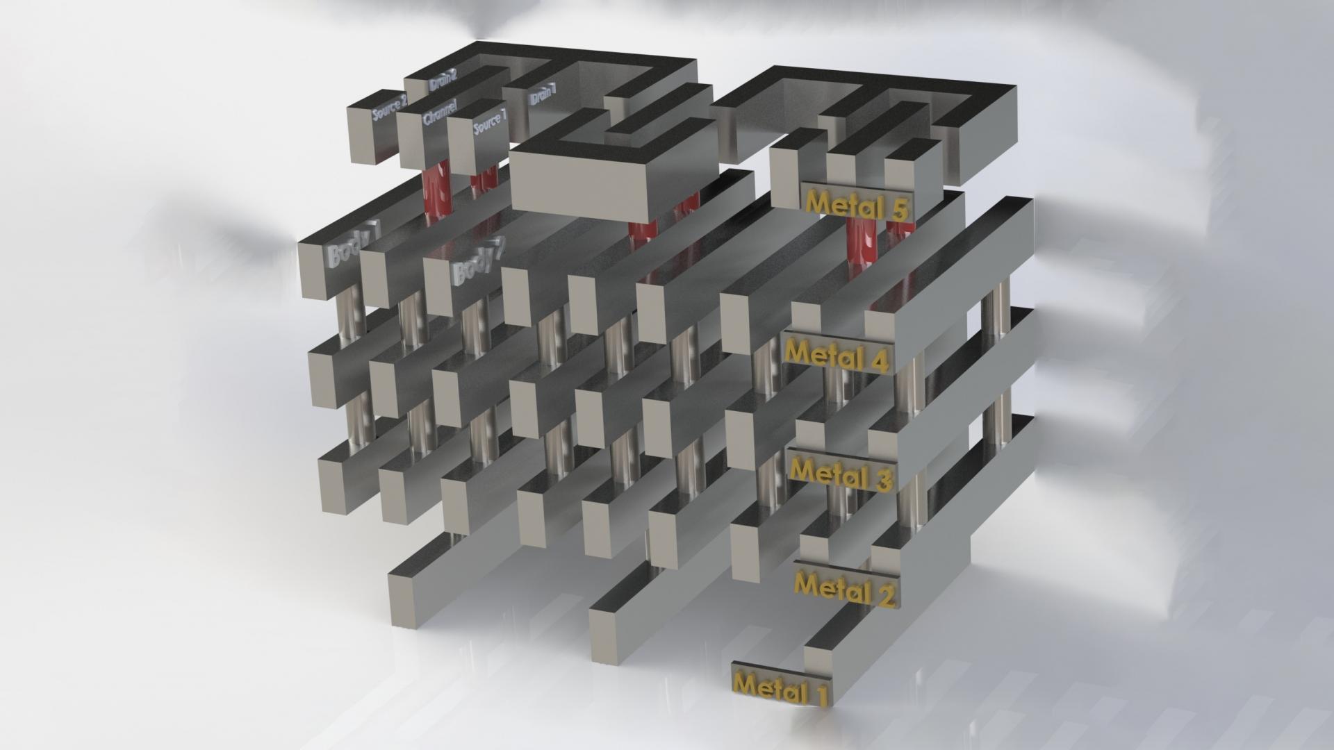
In this collaborative project between KAUST and UC Berkeley, we will leverage the expertise of our teams to investigate a novel nanoelectromechanical (NEM) relay technology for the implementation of robust, reliable and energy-efficient integrated systems. This technology will use an advanced air-gap back-end-of-the-line (BEOL) process, which allows for aggressive scaling of relay footprint and monolithic integration of relay and CMOS devices. A new circuit design paradigm will be developed for the automated implementation of hybrid CMOS-NEM relay integrated circuits (ICs). Such ICs comprise NEM relay logic blocks, analog CMOS blocks, and mixed-mode blocks implemented with both relays and CMOS transistors, such as non-volatile memories, interfaces or data converters. The demonstration of such hybrid integrated systems will be an important milestone toward the adoption of this technology by the semiconductor industry for future IC products.
This effort will include device-level design, modelling, fabrication, and characterization of BEOL NEM relays, circuit/system-level design, synthesis, simulation, implementation, optimization, and testing.
Collaborators
Prof Tsu-Jae King Liu, University of California, Berkeley
