By David Murphy, KAUST News
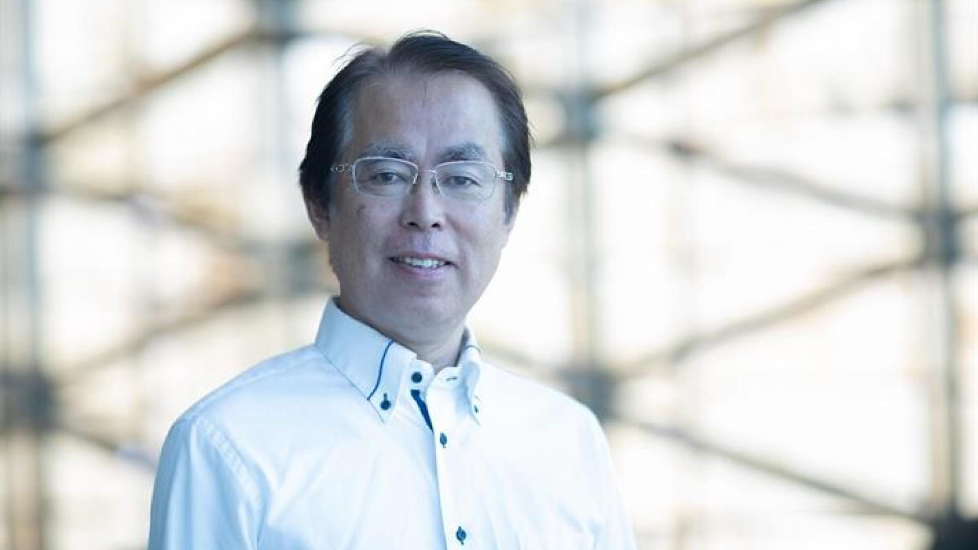
KAUST Professor of Electrical Engineering Kazuhiro Ohkawa was recently elected as a Fellow of the Japan Society of Applied Physics (JSAP). The JSAP was established in 1930 as a voluntary forum for applied physics researchers in the country.
Ohkawa's JSAP peers recognized him for his exceptional contributions to the progression of applied physics and his specific contribution to the "development of wide bandgap semiconductor epitaxial growth and optical devices," JSAP stated.
"It is a great honor for me to be elected as a Fellow of the JSAP," Ohkawa noted. "The Fellowship Award Ceremony will be held as part of the JSAP's Autumn 2019 Meeting. There will be approximately 6,000 participants at the conference. Therefore, it will be a wonderful opportunity for KAUST to promote its reputation to those in Japanese academia."
Contributions to the field of applied physics
Ohkawa's research interests at KAUST focus on the device application of energy-conversion phenomena toward a more sustainable future. As someone who refined the metalorganic vapor-phase epitaxy technique, the highly regarded researcher stated that he first became aware of his contributions to the field of applied physics when he saw how other institutes and industry were utilizing his research.
"I realized my contribution to the field of applied physics when I saw some other institutes [and] companies using the technologies I developed," Ohkawa noted. "In this regard, there are three contributions for my case: the first is doping technologies for II-VI compounds to realize n- and p-types. Those are generally used as the current technologies. Notably, the nitrogen plasma source for the p-type has become the standard technology for MBE [molecular beam epitaxy] growth of nitride semiconductors.
"The second is metalorganic chemical vapor deposition (MOCVD) technology for nitride semiconductors. The technology has developed indium gallium nitride-based RGB full-color LEDs and made it possible to study MOCVD reactors scientifically. The third is the invention of [a] nitride photocatalyst for water splitting and artificial photosynthesis."
"Over 30 industries in Japan, France, Germany, China and Korea have introduced some of those three ideas into their R&D and businesses. It is excellent that our basic academic research can change the world through industries," he continued.
Read the full article

