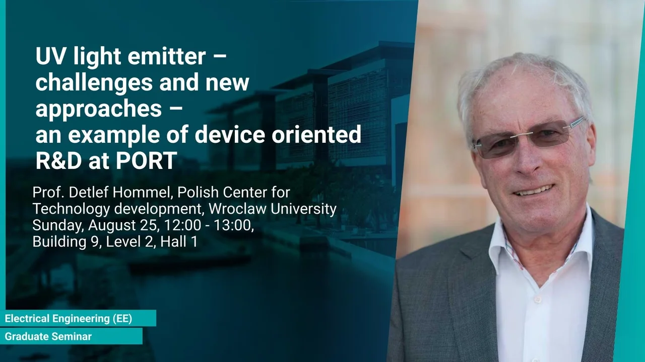
UV light emitter – challenges and new approaches – an example of device oriented R&D at PORT
- Prof. Detlef Hommel, Polish Center for Technology development, Wroclaw University
B9 L2 H1
The Wroław Research Center EIT+ was established in 2007 and renamed in 2018 into Polish Center for technology Development. This year PORT became an institute of the Łukasiewicz Network having similar goals like the Fraunhofer Society in Germany as an applied center for R&D. The presentation will concentrate on my research projects on deep-UV emitters. Going from UV-B (320-280nm) to UV-C (280-200nm) the external quantum efficiency decreases drastically and no breakthrough was obtained here based on high-Al content AlGaN. New, unconventional material combinations are needed to overcome these problems. One idea here is to add a small amount of arsenic to (Al,Ga)N to shift the valence band upwards and to increase the hole concentrations which is crucial for increasing the efficiencies of UV-C emitters. Results will be presented confirming this approach. Another idea is connected with strain engineering by using w-BN. This will allow to shift the unwanted TE to TM transition towards larges bandgaps (higher Al-contents).
Overview
Abstract
The Wroław Research Center EIT+ was established in 2007 and renamed in 2018 into Polish Center for technology Development. This year PORT became an institute of the Łukasiewicz Network having similar goals like the Fraunhofer Society in Germany as an applied center for R&D. The presentation will concentrate on my research projects on deep-UV emitters. Going from UV-B (320-280nm) to UV-C (280-200nm) the external quantum efficiency decreases drastically and no breakthrough was obtained here based on high-Al content AlGaN. New, unconventional material combinations are needed to overcome these problems. One idea here is to add a small amount of arsenic to (Al,Ga)N to shift the valence band upwards and to increase the hole concentrations which is crucial for increasing the efficiencies of UV-C emitters. Results will be presented confirming this approach. Another idea is connected with strain engineering by using w-BN. This will allow to shift the unwanted TE to TM transition towards larges bandgaps (higher Al-contents).
Brief Biography
Prof. Dr. Detlef Hommel is the head of New Materials for Photonics and Electronics, the Polish Center for Technology development (PORT), Poland and a Leopoldina professor at Wroclaw University, Poland. He was a professor at University of Bremen, Germany as a head of Semiconductor Epitaxy at Department of Physics and Electrical Engineering during 1994-2014. He is nominated as a full professor by the Polish President in 2016, a member of the Academia Europeae in 2014, and Alexander von Humboldt Fellow of the Polish Science Foundation FNP during 2006-2009. He organized many international conferences such as 2001 Co-chairman “10th Int’l Conf. on II-VI Compounds” Bremen, Germany; 2005 Chairman “6th Int’l Conf. on Nitride Semiconducturs” Bremen, Germany; 2012 Co-chairman “Int’l Symposium on Light Emitting Structures” Berlin, Germany; 2014 Co-chairman “Int’l Workshop on Nitride Semiconductors” Wroclaw, Poland.
