Taking the heat out of emitters
Semiconductor light-emitting diodes fabricated on a metal substrate are less prone to overheating.
About
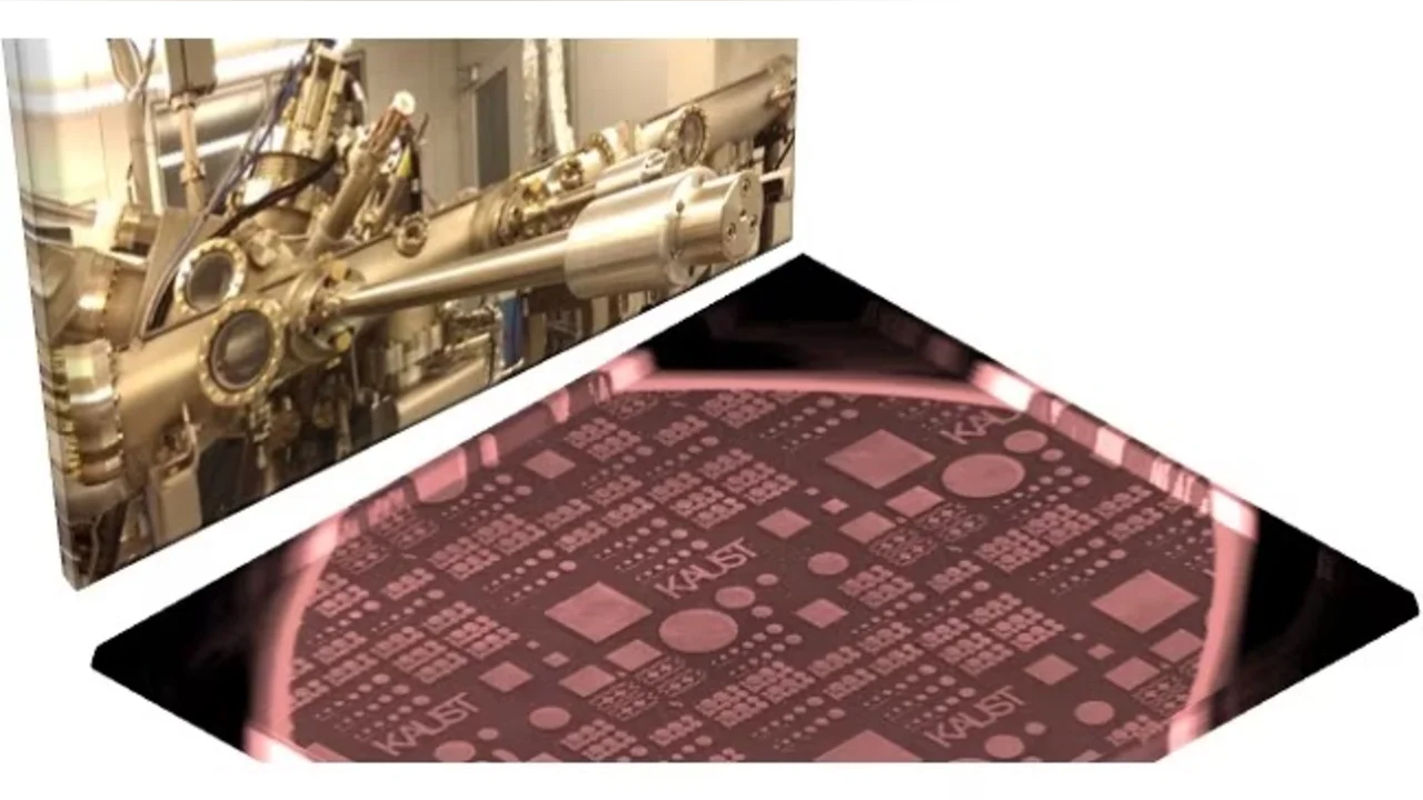
Micrometer-scale light emitters that can be incorporated into electronic chips could enable faster computation and communication systems in compact devices. Researchers at KAUST have developed a simple technique for fabricating optically active semiconductors on a metal substrate, showing that the devices work at room temperature and do not overheat.
The success of the modern electronics industry rests on the ability to fabricate thousands of electronic components on a single silicon chip. Optical devices could benefit in the same way from such an integrated-circuit approach, enabling a cheaper platform for optical communications or portable optical sensors. However, silicon is not the ideal material for optical applications, so an alternative material is required.
Chao Zhao, TienKhee Ng, Boon Ooi and colleagues from the Computer, Electrical and Mathematical Science and Engineering Division used the semiconductor gallium nitride to develop a platform for high-power light emission.
“Nitride-based materials have been intensively studied for photonics applications such as solid-state lighting and displays because the alloys have direct bandgaps that cover the entire visible spectrum,” explained Zhao.
Read the full article.
Related People
Related Researchers

Boon Ooi
- Al-Khawarzmi Distinguished Professor, Electrical and Computer Engineering

Tien Khee Ng
- Principal Research Scientist, Photonics Laboratory