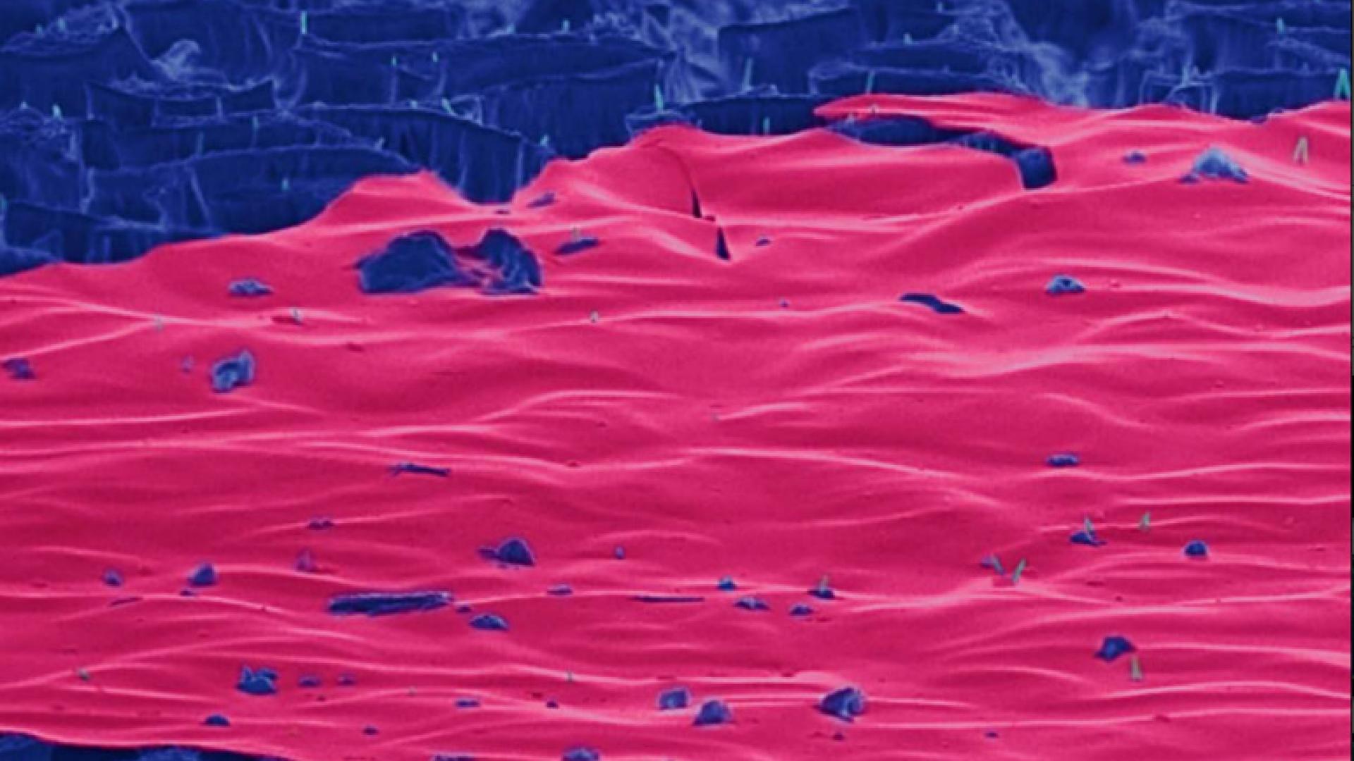
Despite the recent progress in gallium nitride (GaN) growth technology, the excessively high threading dislocation (TD) density within the GaN crystal, caused by the reliance on heterogeneous substrates, impedes the development of high-efficiency, low-cost, GaN-based heterostructure devices. For the first time, the chemical exfoliation of completely TD-free, single-crystalline, ultrathin (tens of nanometers) GaN nanomembranes is demonstrated using UV-assisted electroless chemical etching. These Nano membranes can act as seeding layers for subsequent overgrowth of high-quality GaN. A model is proposed, based on scanning and transmission electron microscopy as well as optical measurements to explain the physical processes behind the formation of the GaN Nano membranes. These novel Nano membranes, once transferred to other substrates, present a unique and technologically attractive path towards integrating high-efficiency GaN optical components along with silicon electronics. Interestingly, due to their Nano scale thickness and macroscopic sizes, these Nano membranes may enable the production of flexible GaN-based optoelectronics.
Collaborators
Rami T. ElAfandy, Mohammed A. Majid, Tien Khee Ng, Lan Zhao, Dongkyu Cha and Boon S. Ooi
Publications
Article first published online: 16 APR 2014 / DOI: 10.1002/adfm.201470104
http://onlinelibrary.wiley.com/doi/10.1002/adfm.201303001/abstract
http://onlinelibrary.wiley.com/doi/10.1002/adfm.201470104/abstract