"A technique developed by scientists at KAUST has made more controlled fabrication of optoelectronic devices produced from a hybrid of organic and inorganic materials possible."
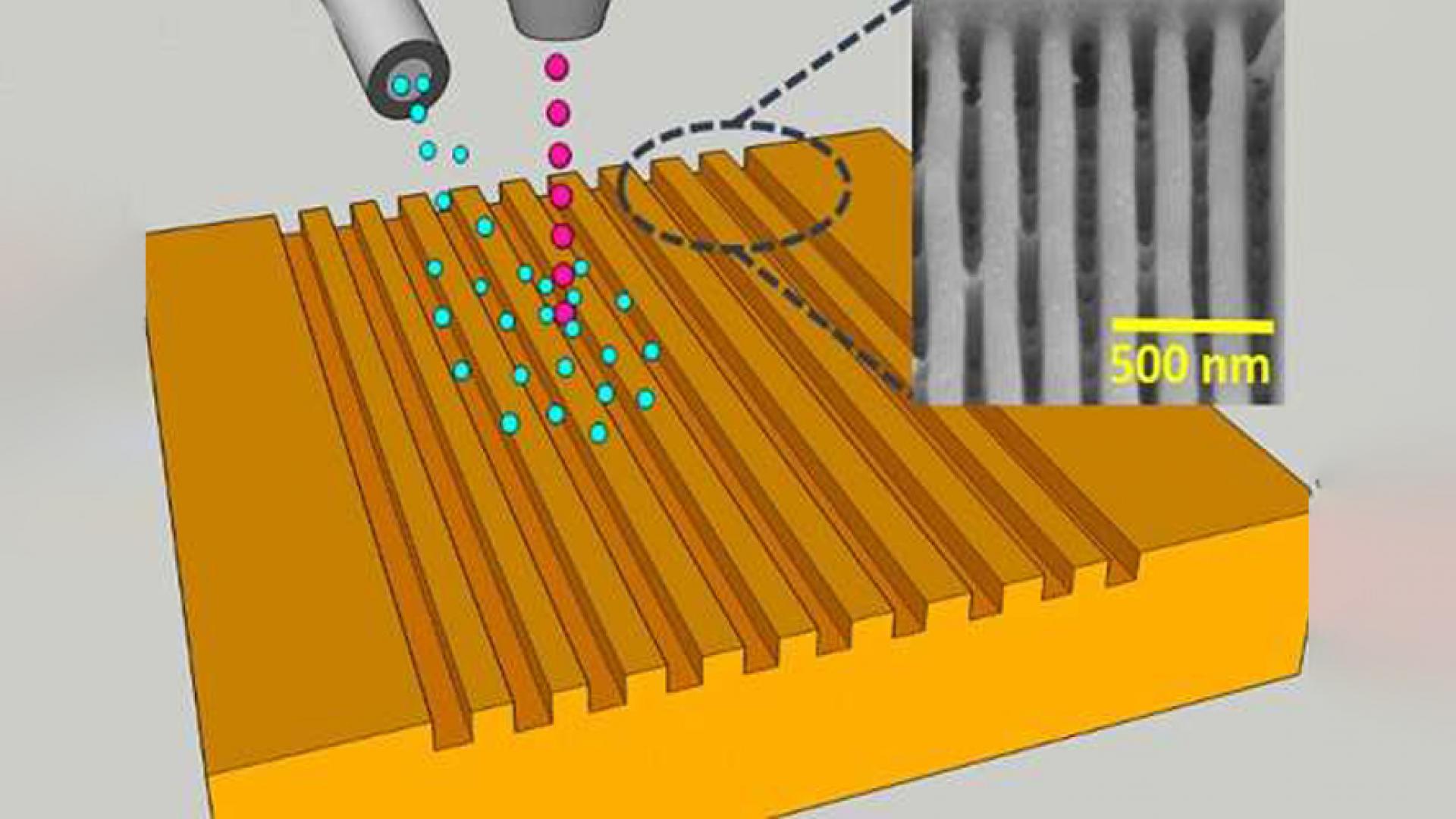
"Ooi and his colleagues from the University's Photonics Laboratory, the Imaging & Characterization Core Lab and the Solar & Photovoltaics Engineering Research Center have demonstrated a technique that can directly pattern perovskites with features smaller than one micrometer with little surface damage."
Using focused-ion beam etching, a grating was created with a trench width of 120 nm separated by 137 nm.
Enhanced Etching, Surface Damage Recovery, and Submicron Patterning of Hybrid Perovskites using a Chemically Gas-Assisted Focused-Ion Beam for Subwavelength Grating Photonic Applications
Mohd S. Alias, Yang Yang, Tien K. Ng, Ibrahim Dursun, Dong Shi, Makhsud I. Saidaminov, Davide Priante, Osman M. Bakr, and Boon S. Ooi
The Journal of Physical Chemistry Letters, 7(1), 137-142 (2016)
Related Persons