ECO Devices Laboratory is developing energy-saving devices and energy-creating devices based on material science. Our tool is MOVPE of Nitrides and Oxides. The leading-edge MOVPE technique is unique in the world. Developing energy-saving devices is a great contribution to the future of society and environment. We are currently focused on the growth of high-quality InGaN and its heterostructures to study carrier and strain behaviors. We can fabricate the world-class LEDs and laser diodes in the yellow and red range.
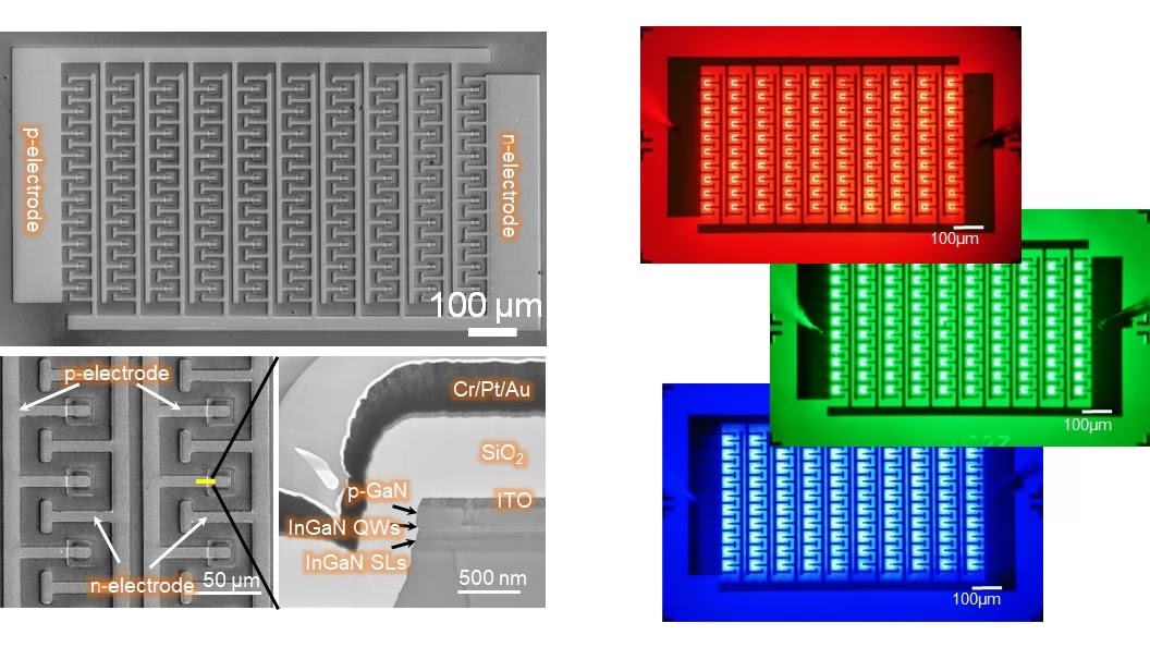
InGaN-based micro-LEDs
Do you know a future display “micro-LED display”? The new display has clear colors, and low power consumption as RGB LEDs are present on the surface without a polarizer. The commercial blue LEDs and green LEDs are made of nitride semiconductors, but the red LEDs are phosphide. We try to realize the alternative material for red LEDs by nitrides.
Reference:
[1] Z. Zhuang, D. Iida, M. Velazquez-Rizo, and K. Ohkawa, "630-nm red InGaN micro-light-emitting diodes (< 20 × 20 µm2) exceeding 1 mW/mm2 for full-color micro-displays", Photonics Research 9, 1796-1802 (2021). DOI: 10.1364/PRJ.428168
Original MOVPE technology for high-quality InGaN
High-temperature InGaN growth is one of the key technologies for covering the entire visible spectrum with light-emitting devices. Our unique MOVPE technique increases the growth temperature by 60oC compared to a typical MOVPE system. We demonstrated the deep-red 740 nm InGaN-based LEDs for the first time.
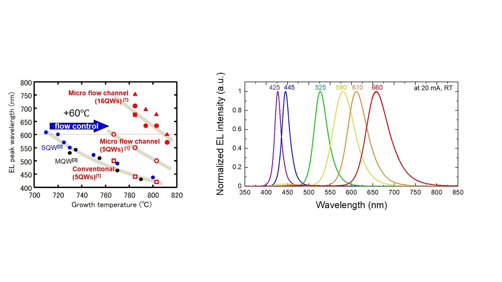
[1] K. Ohkawa, T. Watanabe, A. Hirako, et al., “740-nm emission from InGaN-based LEDs on c-plane sapphire substrates by MOVPE”, Journal of Crystal Growth 343, pp.13-16 (2012).
[2] K. Ohkawa, F. Ichinohe, T. Watanabe, K. Nakamura, D. Iida, "Metalorganic vapor-phase epitaxial growth simulation to realize high-quality and high-In-content InGaN alloys", Journal of Crystal Growth 512, pp.69-73 (2019). DOI: j.jcrysgro.2019.02.018
InGaN-based high-brightness red LEDs
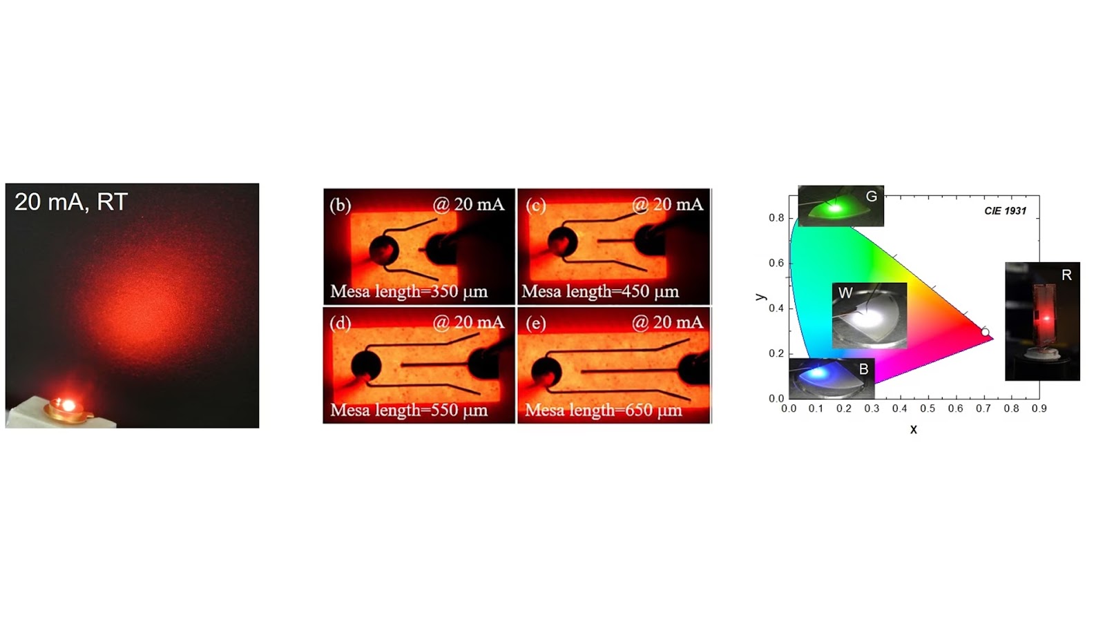
We achieved the InGaN-based red LEDs using our MOVPE technique. In the near future, our red LEDs can contribute realization of RGB-LEDs by only nitrides, the monolithic devices for the micro-LED display are possible. It is a great benefit and breakthrough to fabricate future displays, like VR&AR. The display is energy-saving and environmentally friendly.
[1] D. Iida, Z. Zhuang, P. Kirilenko, M. Velazquez-Rizo, M. A. Najmi, and K. Ohkawa, “633-nm InGaN-based red LEDs grown on thick underlying GaN layers with reduced in-plane residual stress”, Appl. Phys. Lett. 116, 162101 (2020). DOI: 10.1063/1.5142538
[2] Z. Zhuang, D. Iida, and K. Ohkawa, "Effects of size on the electrical and optical properties of InGaN-based red light-emitting diodes", Appl. Phys. Lett. 116, 173501 (2020). DOI: 10.1063/5.0006910
Novel InGaN laser diodes in the yellow and red range
The micro-flow channel MOVPE develops InGaN-based LEDs and LDs. We are challenging to create more efficient InGaN-based LEDs and LDs in the yellow-to-red region to replace phosphides which are explosive materials rather than nitrides. The monolithic nitride solid-state lighting should be safe, efficient and comfortable for our life.
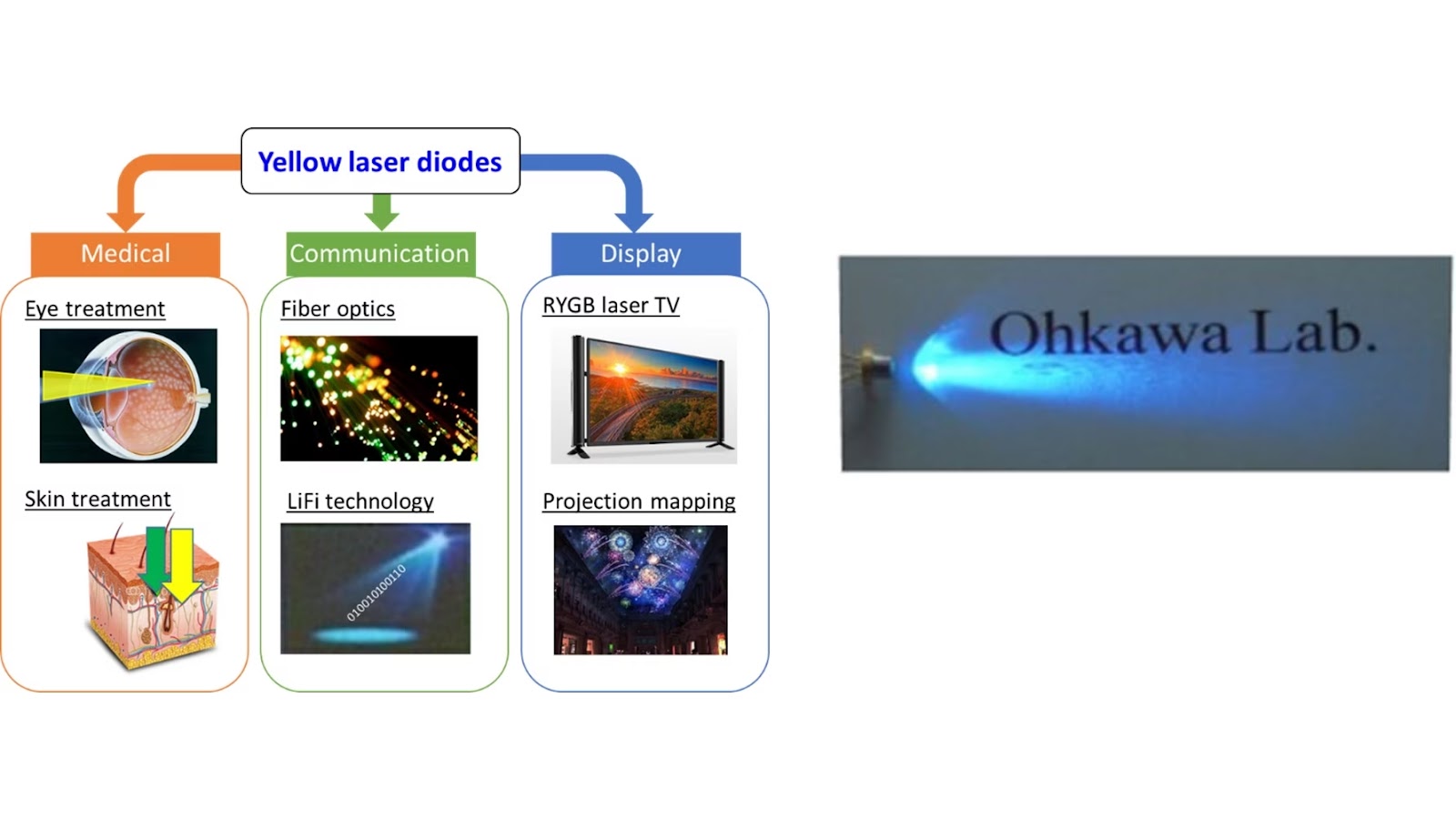
We will develop yellow InGaN lasers. The yellow one is the current missing part of the laser diodes. The yellow region is essential for the medical, communication, and display fields. We can contribute to our great future.
A novel strain compensating technique
The crystal quality of InGaN is very important for optical devices. We have realized that InGaN quantum wells improve the crystalline quality by strain-compensating technique.
InGaN layers are heavily compressively strained. It is important to reduce the strain for suppressing the defect density. This strain-compensating technique is effective in high-In-content InGaN-based devices such as LEDs and LDs. To realize this idea to photocatalysts and solar cells, our further material development is in progress. Further development is necessary to obtain higher-performance devices such as more efficient and/or more powerful.
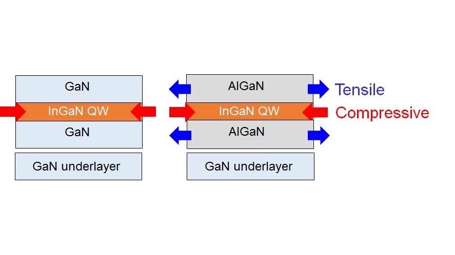

[1] D. Iida, S. Lu, S. Hirahara, K. Niwa, S. Kamiyama, K. Ohkawa, “Investigation of amber light-emitting diodes based on InGaN/AlN/AlGaN quantum wells”, Japanese Journal of Applied Physics 52, 08JB13pp.1-3(2013).
Heterostructure analysis
We are investigating the heterostructure of III-nitrides and oxide materials. The heterostructure analysis by TEM is significantly important for crystal growth. High-resolution TEM can perform the atomical scale observation, which can reveal the strain, composition, and defects in the crystal. Understanding of these informations, we can realize new structures and develop high-performance devices.
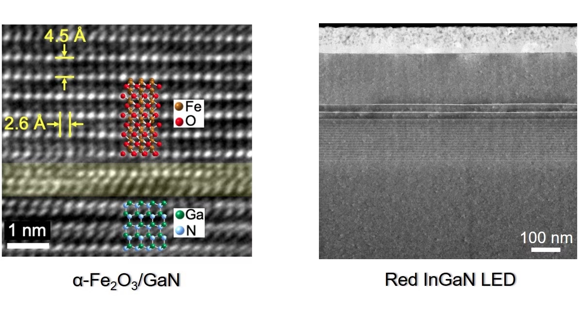
[1] M. Velazquez-Rizo, D. Iida, and K. Ohkawa, "Photoelectrochemical and Crystalline Properties of a GaN Photoelectrode Loaded with α-Fe2O3 as Cocatalyst", Sci. Rep. 10, 12586 (2020). DOI: 10.1038/s41598-020-69419-8
[2] D. Iida, Z. Zhuang, P. Kirilenko, M. Velazquez-Rizo, and K. Ohkawa, "Demonstration of low forward voltage InGaN-based red LEDs", Applied Physics Express 13, 031001 (2020). DOI: 10.35848/1882-0786/ab7168