On 4 Jan., Integrated Photonics Lab (IPL) has published a latest review article on eLight titled “Prospects and applications of on-chip lasers”. The article received plenty of attention in a short period of time and was selected as the cover article of the issue.
Prof. Huiyun Liu's team from UCL has wrote the News & Views about the article and published on Light, titled as "From past to future: on-chip laser sources for photonic integrated circuits". Now is available online.
The following quotes from the EurekAlert! report on this work. (original report page)
Global consumer Internet traffic grew 4-fold from 2017 to 2022 with a compound annual growth rate of 31%. It will reach 4.8 ZB annually by 2022, or 396 Exabytes (EB) per month. Photonic integrated circuits (PICs) are proposed to catalyze powerful new technologies to deal with this ever-growing demand to expand the bandwidth and reduce power consumption.
A team of scientists led by Professor Yating Wan from KAUST and Professor John Bowers from UCSB have published a new paper in eLight that looks at the opportunities of on-chip lasers. They assessed the potential applications in their paper, titled "Prospects and applications of on-chip lasers."
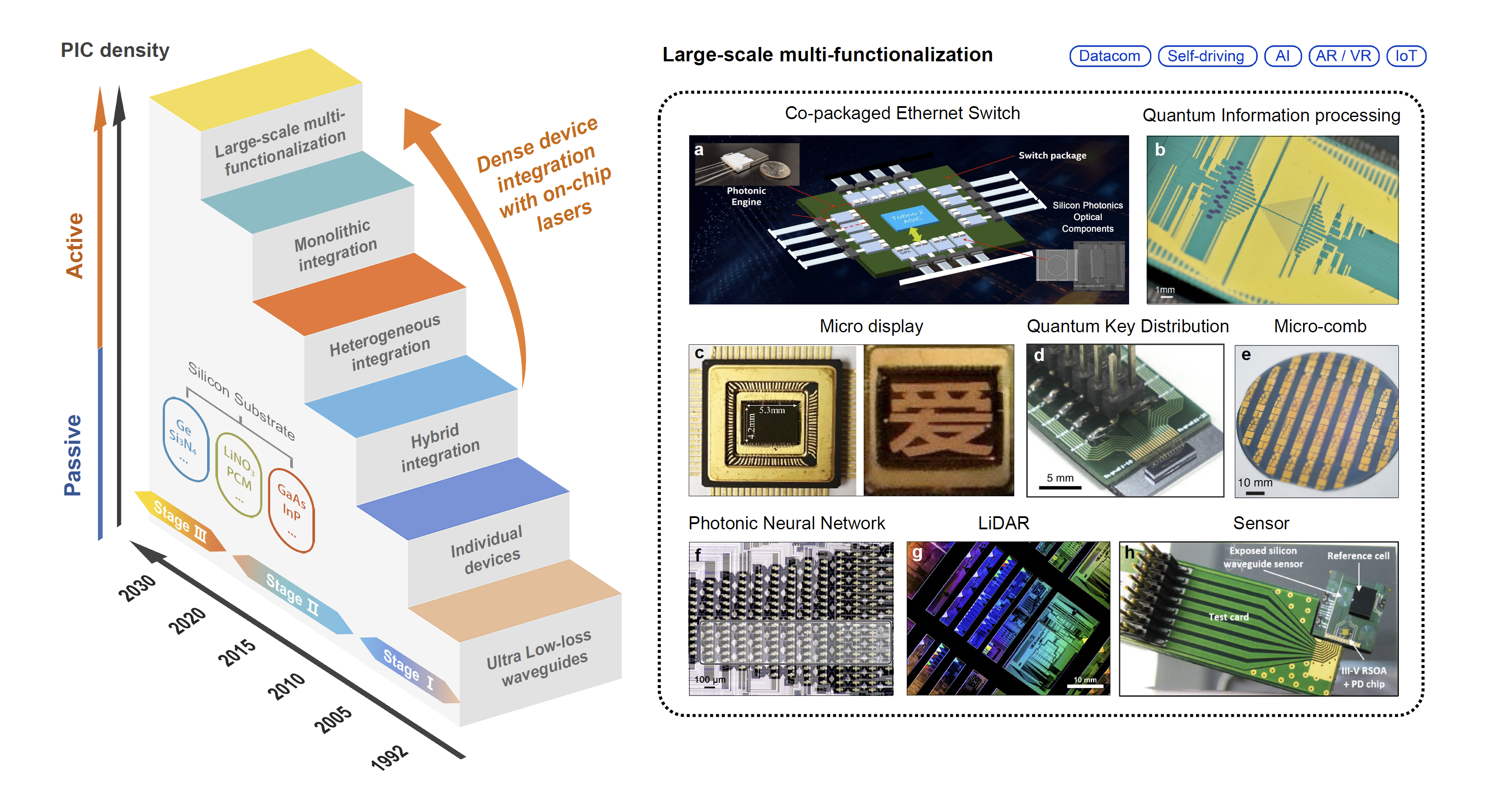
In transitioning from assembled optics to on-chip photonics with compact form factors, silicon becomes an obvious choice due to its superior optical properties and compatibility with the mature complementary metal-oxide-semiconductor (CMOS) technology. The large contrast between silicon and silicon dioxide allows photonic devices to be fabricated in a compact size. The range of optical components demonstrated on the silicon-on-insulator (SOI) platform is extremely impressive. However, silicon has a low emission efficiency. On-chip light sources lagged far behind silicon-based photonic devices and became a bottleneck for mass production. To break a barrier, a great deal of research has emerged in the field of on-chip light sources in the past decades. In this review, the authors focus on the on-chip integration of the key element in PIC: a compact, energy-efficient, and robust laser source. They start with an overview of the decades of efforts in exploring new materials and integration technologies for on-chip lasers, including hybrid, heterogeneous, and monolithic integration.
Over 6 million 100-gigabit optical modules with heterogeneously integrated on-chip lasers have been shipped by Intel, generating over $1 billion of revenue. In monolithic integration, significant improvements in III-V/Si epitaxy have pushed quantum dot (QD) technology to the frontiers of silicon photonics. The large tolerance to material defects allows for efficient device operation despite the material incompatibility between silicon and III-V. The much-reduced reflection sensitivity feedback offers the prospect of eliminating optical isolators in PICs. These lasers' record-low threshold currents and high temperature stability offer many new possibilities.
Several paths have also been explored for active-passive coupling and co-integration of QD lasers to the other parts of silicon photonics. A monolithic offset QD integration platform has been established, permitting the formation of a laser cavity utilizing both the robust QD active region and the versatility of passive GaAs waveguide structures.
A heterogeneous QD integration platform is showing very promising results. A synergistic relationship between the III-V QDs and silicon gives rise to superior devices exceeding what is achievable with purely III-V QD devices. With lifetimes entering the realm of commercial relevance, this approach promises to scale photonic integrated circuits to 300 mm or even 450 mm diameter wafer size for high volume applications.
The biggest driver in further development of silicon photonics is still datacom. However, dense device integration with on-chip lasers will be critical for several envisioned future applications.
In the second part of the review, the authors analyze the corresponding material system compatibility and efficient energy channeling from device to device on-chip. The review focuses on the benefits and potential implementation of on-chip lasers in various functionalized PICs, including optical communications and interconnects, optical phased array-based LiDAR, chemical and biological analysis, and sensors.
The prospect of silicon photonics and silicon integrated circuits was undeniably too compelling. It is owed chiefly to their ability to use and seamlessly integrate with the already matured high-quality CMOS fabrication technology. CMOS fabrication technology can achieve high-volume yields at low die-costs, in addition to excellent uniformity and a large degree of scalability. An abundance of research and development from academia and the industry has resulted in multiple solutions to surmount shortcomings over the years. As time progressed, new approaches have been increasingly conceived. Indeed, various chip-level devices have matured today based on silicon photonic processes for various applications incorporating on-chip lasers by the different integration techniques. However, major manufacturers' design and process routes still vary significantly. From this point of view, PIC technology is still in its infancy, where the ultimate solution with the optimal cost-performance-reliability balance has yet to stand out from the crowd.
Related Persons