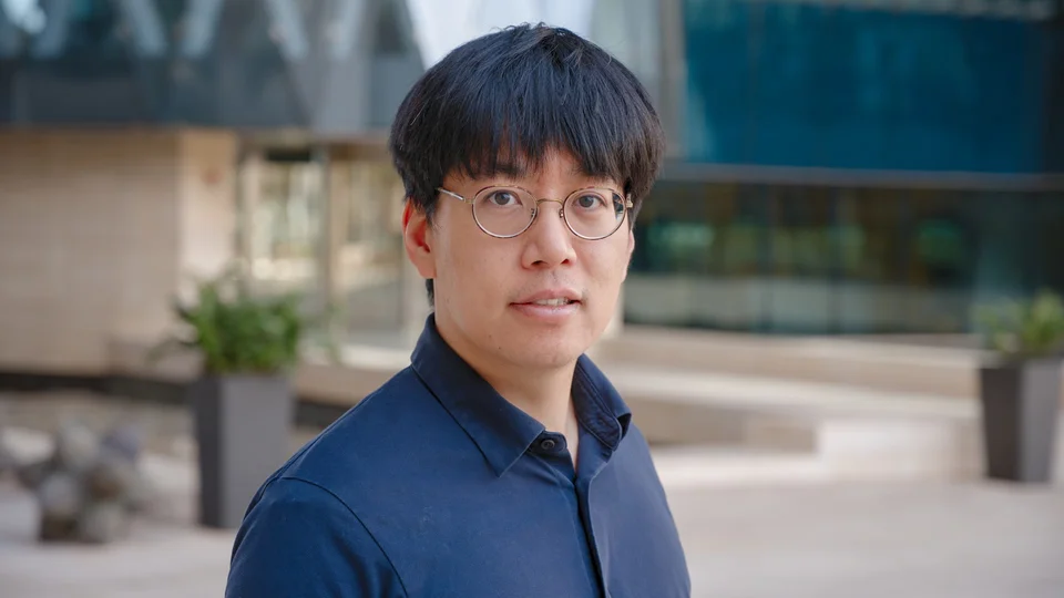
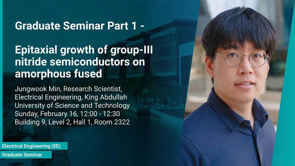
About Jung-Wook Min Jung-Wook Min Research Scientist, Photonics Laboratory nanomaterials GaN Photonics and optoelectronics molecular beam epitaxy Large bandgap group-III nitride Introduction Jung-Wook Min is a Research Scientist at Photonics Laboratory in the Division of Computer, Electrical and Mathematical Science and Engineering (CEMSE) at King Abdullah University of Science and Technology (KAUST). He received his M.S. and a Ph.D. degree in the Department of Physics and Photon Science at Gwangju Institute of Science and Technology (GIST), Republic of Korea, in 2012 and 2016. He has 10 years of hands-on experiences of refurbishment, modification and maintenance of various type of III-N and III-As/P MBE chambers and has been focused on the epitaxial growth of III Events Presented Events Feb 16 - Feb 22, 2020 Epitaxial growth of group-III nitride semiconductors on amorphous fused silica glass and its heterogeneous integration for optoelectronic devices Jung-Wook Min, Research Scientist, Photonics Laboratory Feb 16, 12:00 - 12:30 B9 L2 H1 R2322 Graduate Seminar Part 1. In this talk, catalyst- and mask-free GaN nanowires ensemble were grown by plasma-assisted molecular beam epitaxy (PA-MBE) under nitrogen-rich condition. Prior to optoelectronic device realization, we conducted fundamental studies including diffusion-induced growth mechanisms on various substrates. On bare fused silica substrate, without any buffer layer, hundreds-of-nanometer scale grains of GaN nanowires were examined by SEM and interfaces were investigated by TEM. Despite the poly-crystalline properties of the coalescent columnar GaN layer, each grain showed the preferential orientation along the c-axis growth direction. To provide conductivity and transparency on amorphous fused silica as a thermally durable substrate, transparent conductive oxide (TCO) layers were deposited by RF magnetron sputtering method on a fused silica glass substrate. Next, for the heterogeneous integration toward solar cell application, we introduced n-GaN nanowires as an electron transport layer (ETL) for methylammonium lead iodide (MAPbI3) perovskite solar cells (PSCs). n-GaN nanowires showed high electron mobility and UV blocking characteristics with MAPbI3. Moreover, finite-difference time-domain (FDTD) simulation confirmed that the roughened interfaces of GaN nanowire arrays are helpful for photon recycling. These achievements can open a new pathway for the heterogeneous integration of group-III nitride and perovskite semiconductors and substrate-independent epitaxy.
Epitaxial growth of group-III nitride semiconductors on amorphous fused silica glass and its heterogeneous integration for optoelectronic devices Jung-Wook Min, Research Scientist, Photonics Laboratory Feb 16, 12:00 - 12:30 B9 L2 H1 R2322 Graduate Seminar Part 1. In this talk, catalyst- and mask-free GaN nanowires ensemble were grown by plasma-assisted molecular beam epitaxy (PA-MBE) under nitrogen-rich condition. Prior to optoelectronic device realization, we conducted fundamental studies including diffusion-induced growth mechanisms on various substrates. On bare fused silica substrate, without any buffer layer, hundreds-of-nanometer scale grains of GaN nanowires were examined by SEM and interfaces were investigated by TEM. Despite the poly-crystalline properties of the coalescent columnar GaN layer, each grain showed the preferential orientation along the c-axis growth direction. To provide conductivity and transparency on amorphous fused silica as a thermally durable substrate, transparent conductive oxide (TCO) layers were deposited by RF magnetron sputtering method on a fused silica glass substrate. Next, for the heterogeneous integration toward solar cell application, we introduced n-GaN nanowires as an electron transport layer (ETL) for methylammonium lead iodide (MAPbI3) perovskite solar cells (PSCs). n-GaN nanowires showed high electron mobility and UV blocking characteristics with MAPbI3. Moreover, finite-difference time-domain (FDTD) simulation confirmed that the roughened interfaces of GaN nanowire arrays are helpful for photon recycling. These achievements can open a new pathway for the heterogeneous integration of group-III nitride and perovskite semiconductors and substrate-independent epitaxy.
Related Sites Electrical and Computer Engineering (ECE) Photonics Laboratory (Photonics) Related Content Articles 2 Events 1