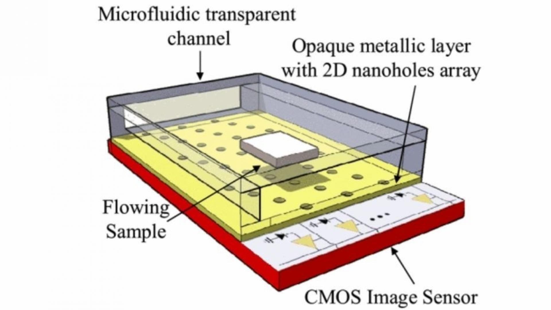
Recently, a novel optical imaging device which is directly integrated into a microfluidic channel and achieves submicron imaging resolution comparable to that of conventional microscopes was reported by Yang and others and termed Optofluidic Microsopy (OFM). This new compact imaging device functions as a lab-on-a-chip to capture very high resolution images of biological samples flowing in microfluidic channels. OFM system offers many advantages, among them: miniaturized design, low cost, high throughput, and nondestructive optical probing. But the key advantage of OFM is its ability to capture high (submicron) resolution images although it is free from any conventional optical lenses. Instead of resorting to bulky optics, OFM is based on optical sensing through a linear nanoholes array that is defined in an opaque metallic layer, patterned onto the bottom of the microfluidic channel and mounted on top of a linear image sensor. because of this nanoholes array, OFM imaging resolution becomes completely independent of the image sensor pixel’s size.
The first reported design of OFM system requires some modifications for real time operation. We suggested previously the utilization of 2D nanoholes array in OFM system to achieve a real time OFM device with acceptable frame rate. We modeled the structure of the real time OFM strucutre using a numerical optical simulator that is based on the finite element method to verify its operation. Our simulation results revealed some problems for the implementation of 2D nanoholes array in a single metal layer at the surface of the chip. So we presented a novel structure that solves all these problems and even offers more advantages by minimizing the required fabrication steps of the device.
- T. Elkhatib, Z. Huang and KN Salama, ‘Real Time Optofluidic Microscopy ,’ IEEE NEWCAS, Montreal, Canada, June 2008 [accepted to be published]
- T. A. Elkhatib and K. N. Salama, “Super-Resolution: Imaging beyond the Pixel Size Limit,” IEEE Custom Integrated Circuits Conference (CICC), San Jose, CA, USA, Sept. 2008, pp.515-518.
- T. A. Elkhatib and K. N. Salama, “Nanoholes Microscopy,” IEEE Asia Pacific Conference on Circuits and Systems (APCCAS), Macao, China, Dec. 2008, pp 360-363.
- T. A. Elkhatib, K. N. Salama, “High resolution imaging through integrated nanoholes image sensor,” IEEE Biomedical Circuits and Systems Conference (BioCAS), Baltimore, MD, USA, Nov. 2008, pp. 245-248. (Poster Presentation)
- T. A. Elkhatib, Z. Huang and KN Salama, “Real Time Optofluidic Microscopy,” the Joint 6th International IEEE Noertheast workshop on circuits and systems and TAISA conference (NEWCAS-TAISA), Montreal, QC, Canada, Jun. 2008, pp. 53-56.
This material is presented to ensure timely dissemination of scholarly and technical work. Copyright and all rights therein are retained by authors or by other copyright holders. All persons copying this information are expected to adhere to the terms and constraints invoked by each author's copyright. In most cases, these works may not be reposted without the explicit permission of the copyright holder. ©20xx IEEE. Personal use of this material is permitted. However, permission to reprint/republish this material for advertising or promotional purposes or for creating new collective works for resale or redistribution to servers or lists, or to reuse any copyrighted component of this work in other works must be obtained from the IEEE.