Abdullah Almansouri, et al., "A Dual-Mode Nested Rectifier for Ambient Wireless Powering in CMOS Technology." IEEE Transactions on Microwave Theory and Techniques, 68 (5), 2020, 1754.
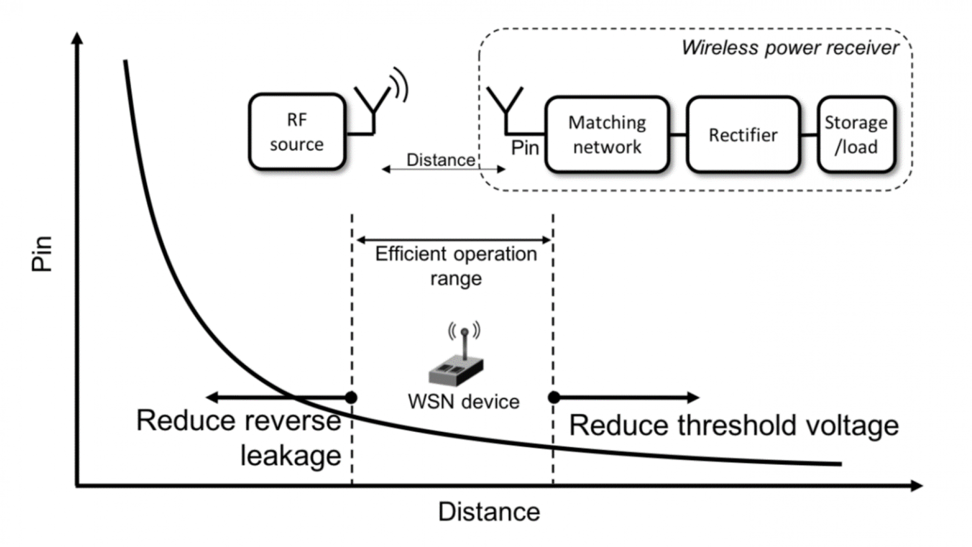
This article proposes (DM) nested radio frequency (RF) rectifier for ambient wireless powering. The proposed architecture utilizes a DM nested feedback circuit to enhance the conductivity of the rectifier at low power while reducing the reverse leakage current at high power by generating supply voltages at the gates of the pMOS rectifying transistors. The proposed rectifier is fabricated in a 65-nm CMOS technology and occupies an area of 6480 μm². The measurement results show a peak power conversion efficiency of 86%, 10.1-dB dynamic range, and -19.2-dBm 1-V sensitivity when operating with a 100-kΩ load at the industrial, scientific, and medical band 433 MHz. Moreover, the enhanced low-power performance is achieved by reducing the effective threshold voltage of the rectifier by about 37%, compared with a low-threshold transistor in the 65-nm technology. This reduction in the threshold voltage allows the rectifier to operate with efficiency exceeding 10% for input power ≥ -40 dBm
.