Event Start
Event End
Location
Abstract
Silicon has been the cornerstone of the electronics industry for decades with its unmatched material quality and device performance. However, its intrinsic limitations, particularly its narrow bandgap energy, hinder its efficacy in high-power and extreme environmental applications such as elevated temperatures and radiation exposure.
Ultra-wide bandgap (UWBG) semiconductors, such as Gallium Oxide (Ga2O3) with a bandgap energy (Eg) of 4.8 eV and Aluminum Nitride (AlN, Eg = 6.2 eV), present a potent alternative for these specialized applications owing to their inherently larger bandgap energies. However, the lack of p-type doping capabilities in UWBG materials precludes the implementation of conventional CMOS inverters.
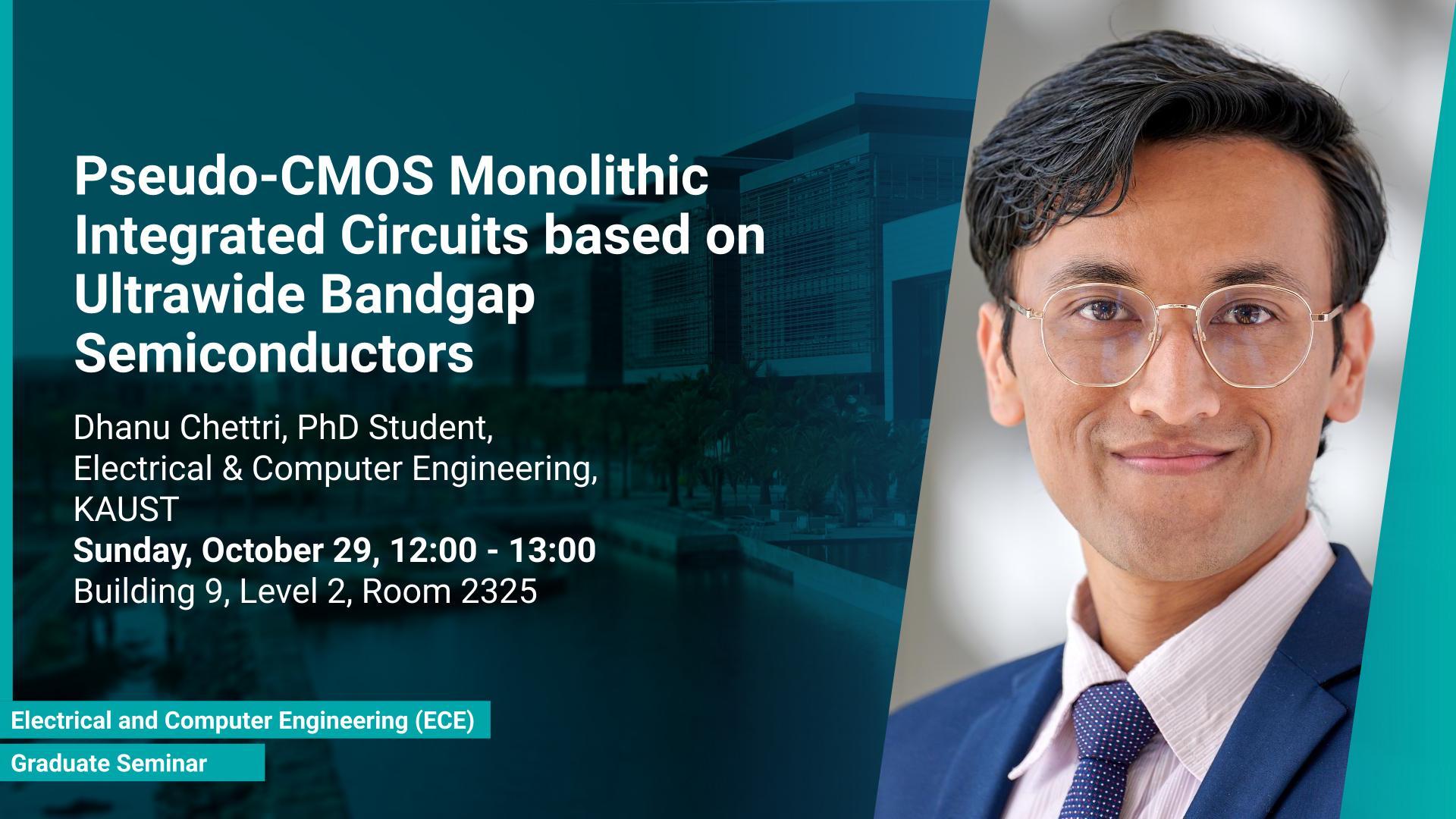
This talk presents a pioneering approach to mitigate this drawback by introducing a pseudo-CMOS inverter fabricated in Ga2O3. Key contributions include the successful fabrication of Ga2O3-based pseudo-CMOS monolithic inverter integrated circuits (ICs) and their stable operation at temperatures as high as 250°C. This seminar will articulate the growth, and fabrication methodologies employed, discuss the device characterization under high-temperature conditions, and extrapolate on the far-reaching implications of these advancements for the realm of electronics designed to operate under extreme environmental conditions.
Brief Biography
Dhanu Chettri is a Ph.D. student at the Advanced Semiconductor Laboratory (ASL), KAUST under the mentorship of Prof. Xiaohang Li. He specializes in studying ultra-wide bandgap semiconductors, focusing on Gallium Oxide (Ga2O3) and Aluminum Nitride (AlN).
Before joining KAUST, he was a senior project fellow at the Council Of Scientific And Industrial Research–Central Electronics Engineering Research Institute (CSIR–CEERI). Chettri has an interdisciplinary approach that spans from material growth to micro and nano-fabrication. Their research majorly centers around the design, fabrication, and circuit implementation of transistors such as MOSFETs.
He has contributed to the field through impactful research articles, including a notable paper on "β-Ga2O3 Pseudo-CMOS Monolithic Inverters," published in IEEE Transactions on Electron Devices. His work holds particular promise for applications in high-temperature and extreme environments electronics, highlighting the versatility and utility of ultra-wide bandgap semiconductors.
