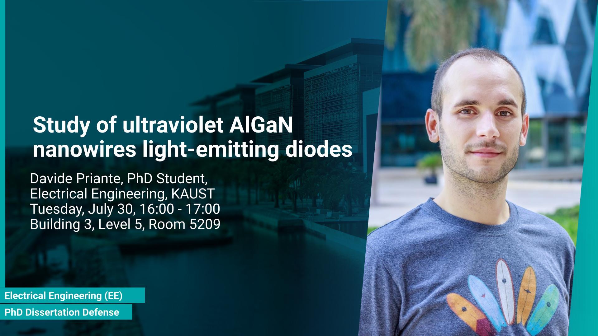
Event Start
Event End
Location
Abstract
Ultraviolet (UV) group III-Nitride-based light emitters have been used in various applications such as water purification, medicine, lighting and chemical detection. Despite attractive properties such as bandgap tunability in the whole UV range (UV-C to UV-A), high chemical stability and relative low cost, the low quantum efficiency hamper the full utilization. In fact, external quantum efficiencies of UV devices are below 10 % for emission wavelength shorter than 350 nm.
This thesis aims to show alternative solutions to such problems by employing nanowires (NWs) structures, and target the eventual application of reliable and high power NWs-based light-emitting devices, enabling large-scale production using the established silicon foundry processes. Here, we present the improvement of injection current and optical power of AlGaN NWs LEDs by involving a metal bilayer thin film with a dual purpose: eliminate the potential barrier for carrier transport, and inhibit the formation of silicide.
We then study the AlGaN/GaN UV LED design to optimize the device structure and improve the LED performance. We compared multiple devices having different active region and graded layers’ thicknesses. Improvement on the output power was achieved for larger p-AlGaN graded layer and thinner p-GaN contact layer structure due to the better hole injection and lower p-GaN absorption.
The junction temperature of AlGaN-based NWs LEDs on metal bi-layer and silicon is also presented as a crucial parameter affecting the device efficiency, chromaticity and reliability. In this regard, by using the forward-voltage and peak-shift method we extracted the junction temperature values and confirmed the better heat dissipation in NWs grown on metal substrate.
Finally, the origin of single and ensemble NWs current injection and injection efficiency are studied by treating the AlGaN NWs with KOH solution. Measurements based on conductive atomic force microscopy enabled a fast feedback cycle without fabricating the device.
Despite the NWs technology is still at its infancy compared to the matured planar, we believe that this research effort will give important insight in advancing the AlGaN NWs devices for future industrial employment.
Brief Biography
Davide received his B.Sc. degree in Material Science Engineering from University of Padova, Italy, in 2013. He joined KAUST in February 2014 as an MS-to-PhD student in Photonics Laboratory in the Computer, Electrical and Mathematical Sciences & Engineering (CEMSE) Division where he is currently pursuing his PhD degree.
His research topic focuses on enhancing the performance of large bandgap ultraviolet III-nitride semiconductor nanostructured light emitters. It involves the device structure design optimization and the usage of highly conductive thin metal substrates.