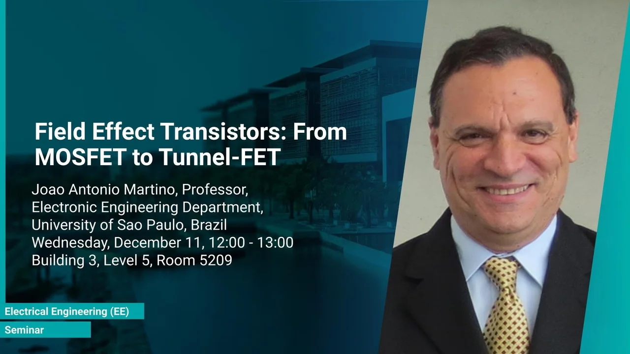
Field Effect Transistors: From MOSFET to Tunnel-FET
The Field Effect Transistor (FET) is the main device for the integrated circuits era. This presentation starts with an overview of the main progress steps of FET evolution and finish with a discussion of possible FET devices for future technologies. New type of device conduction mechanism like Tunnel-FET devices (TFETs) have been studied to replace the conventional drift-diffusion conduction mechanisms due to the benefits obtained by tunneling conduction. The analog behavior of the TFET device will be presented. Nanowire devices and the first basics circuits with Tunnel-FET will be discussed and compared with FinFET ones.
Overview
Abstract
The Field Effect Transistor (FET) is the main device for the integrated circuits era. This presentation starts with an overview of the main progress steps of FET evolution and finishes with a discussion of possible FET devices for future technologies. The starting point was the Lilienfeld patent filled in 1925 that was not fabricated due to technological difficulties. Experimental Metal-Oxide-Semiconductor FET (MOSFET) was only obtained in 1960. The classical MOSFET was composed of Aluminum (Metal), silicon dioxide (Oxide) and Silicon (Semiconductor). In order to follow Moore´s Law evolution and to avoid the short channel effects the classical MOSFET has to be upgraded using new materials and new device structures in order to improve the electrostatic control between gate and channel. The MOSFET has been upgraded with different gate electrodes like polysilicon heavily doped, TiN and TaN. The gate oxide has also been replaced to high-k dielectrics like SiON, HfSiON, and $HfO_{2}$ in order to avoid gate leakage current. Finally, the well-known silicon channel has also been modified to strained silicon (uniaxial and biaxial), SiGe, Ge, InGaAs in order to boost the carriers' mobility. The MOSFET structure has been improved from Bulk MOSFET to SOI (Silicon-on-Insulator) MOSFET and later from planar to vertical multiple-gate devices like FinFET, Triple Gate and Gate all-around devices for enhancing the electrostatic coupling. A new type of device conduction mechanism like Tunnel-FET devices (TFETs) has been studied to replace the conventional drift-diffusion conduction mechanisms due to the benefits obtained by tunneling conduction. The analog behavior of the TFET device will be presented. Nanowire devices and the first basics circuits with Tunnel-FET will be discussed and compared with FinFET ones.
Brief Biography
Joao Antonio Martino was born in Sao Paulo, Brazil, preserving both nationalities: Brazilian and Italian. He starting on the microelectronics field since 1982 on a graduate program, when he received the Master (NMOS technology) and the Ph.D. (CMOS technology) degrees in 1984 and 1988, respectively, in Electrical Engineering (microelectronics area) from University of Sao Paulo (USP), Brazil. He worked as a post-doctoral researcher in a joint collaboration between Imec (Inter-University Microelectronic Center) / KU Leuven (University of Leuven), Belgium and University of Sao Paulo, from 1989 to 1994 in SOI technology and devices.
He is a Full Professor since 2005 and head of CMOS SOI group since 1990 at the Electrical Engineering Department of the University of Sao Paulo, Brazil. He was also the head of the Electrical Engineering Department at the University of Sao Paulo from 2009 to 2013. He is author and co-author of more than 500 technical journal papers and conference proceedings and author/editor of 7 books. He concludes the advisor work of 51 students (19 Ph.D. and 32 master students). He introduced the study of SOI devices characterization and technology in Brazil in 1990. His expertise is in the area of the electrical characterization, simulation and modeling of SOI devices at low/high temperatures, strain and radiation environment. He is also interested in the SOI-CMOS fabrication process and Multiple Gate devices. He was the head of the first 3D transistor (triple gate FinFET) fabricated in South America in 2012.
Recently he is working on Tunnel-FETs in collaboration between the University of São Paulo and Imec/Belgium and UTBB SOI (Ultra-Thin Body and Buried oxide) and nanowire devices in collaboration with MINATEC, Grenoble. He is a Senior Member of IEEE, Member of Electrochemical Society. He has been Chapter Chair of South Brazil Session of IEEE – Electron Device Society (EDS) since 2007 and Distinguished Lecturer of EDS/IEEE since 2008. He is also Vice-Chair of Region 9 Subcommittee for Regions/Chapters (SRC) EDS/IEEE since 2011.
