The wide bandgap semiconductor has been revolutionizing the human society in numerous aspects, including energy, food, water, environment, and information. Our research aims to investigate fundamental science and create more cutting-edge technologies for a better world and future.
Website
Xiaohang Li is an Associate Professor of Electrical and Computer Engineering (ECE) and Principal Investigator of the Advanced Semiconductor Lab. Li’s has conducted multidisciplinary research projects related to solid state lighting, colloidal particles, ferromagnetic fluid, and water purification at various research organizations. Currently, Li’s research focuses on growth, fabrication and characterization of III-nitride semiconductors for optoelectronic and electronic devices.
Areas of expertise and current scientific interests
Professor Li is interested in the ultrawide bandgap and wide bandgap semiconductors. He is focused on growth, simulation, fabrication, and characterization of next-generation III-nitride and III-oxide devices. Professor Li's research has resulted in many pioneering and cutting-edge results widely recognized and awarded by IEEE, SPIE, American Association of Crystal Growth, and Edison Innovation Foundation.
The devices of particular interest include LED, laser, high power devices, high frequency devices, and sensors. These devices are expected to become the enabling technologies to revolutionize energy, communication, health, sensing, and many others which are crucial for the sustainable future of human society.
Professor Li's research activities are highly interdisciplinary. They involve students and researchers from electrical engineering, applied physics, material science, machine learning, and other related disciplines. They are supported by state-of-the-art facilities including and not limited to: MOCVD, PLD, ALD, photolithography, e-beam lithography, PL, TEM, XRD, Raman, XPS, SIMS, RBS, supercomputer in his lab and at KAUST.
Why wide bandgap semiconductors?
Semiconductor technology is arguably the most important technology which transforms the human beings into the digital age today. From homes, companies, organizations, government, to outer space, there are trillions of semiconductor devices empowering every aspect of the society.
The wide bandgap semiconductor is an emerging branch of the overall semiconductor field. It has unparalleled material properties that can be made into cutting-edge solid state ultraviolet to infrared light sources, solar cells, high power devices, high-frequency devices, and sensors. One of the good examples is GaN LED which produces nearly all the light in the evenings at KAUST and in many places all over the world. The Nobel Prize in Physics 2014 is a direct result of R&D in GaN LED. However, it is just the beginning for the wide bandgap semiconductors. There are still enormous research and commercialization opportunities for anyone who is working in the field. Because of its importance, the wide bandgap semiconductor is often referred to as the third generation semiconductor. My group is all into discovery new science and develop cutting-edge technologies in this promising field.
Why KAUST?
I was attracted to KAUST because KAUST offers strong support so that I can build a world-class lab and spend sufficient quality time advising students and discussing ideas. KAUST also has some of the best students, postdocs, scientists, and faculty in the world. Working with them is a great pleasure and blessing for me. Saudi Arabia is also transforming into a modern society, leading to numerous opportunities—I have witnessed a similar process in China since the 1980s, with huge opportunities generated for the people. KAUST is also such a beautiful place, with the Red Sea just steps away—the campus is perfectly designed, making commuting, living and working a great pleasure. Every day I am learning new ideas and knowledge from discussions, seminars, and conferences on campus. I have also had ample opportunities to travel to different conferences and institutions to build academic connections and collaborations.
Curriculum Vitae
Selected Publications
For the complete list and PDF paper files, please visit the "Publications" tab or Google Scholar.
1. "Graded-Index Separated Confinement Heterostructure AlGaN Nanowires: Towards Ultraviolet Laser Diodes Implementation," ACS Photonics. 5, 3305 (2018).
2. "Lateral-Polarity-Structure of AlGaN Quantum Wells: A Promising Approach for Enhancing the Ultraviolet Luminescence," Advanced Functional Material 28, 1802395 (2018).
3. “Tapering-induced enhancement of light extraction efficiency of nanowire deep ultraviolet LED by theoretical simulations,” Photonics Research 6, 124 (2018).
4. "HCl flow-induced phase change of α-, β- and ε-Ga2O3 films grown by MOCVD," Crystal Growth & Design 18, 2370 (2018).
5. "Surface-Passivated AlGaN Nanowires for Enhanced Luminescence of Ultraviolet Light Emitting Diodes," ACS Photonics 5, 964 (2018).
Publications
Education Profile
- Ph.D., Electrical Engineering minor in Physics, Georgia Institute of Technology
- M.S., Electrical Engineering, Lehigh University
- B.S., Applied Physics, Huazhong University of Science and Technology
Awards and Distinctions
- News Features, Semiconductor Today, 2019
- IEEE North Jersey Section ED/CAS MTT/AP Chapters Award, 2019
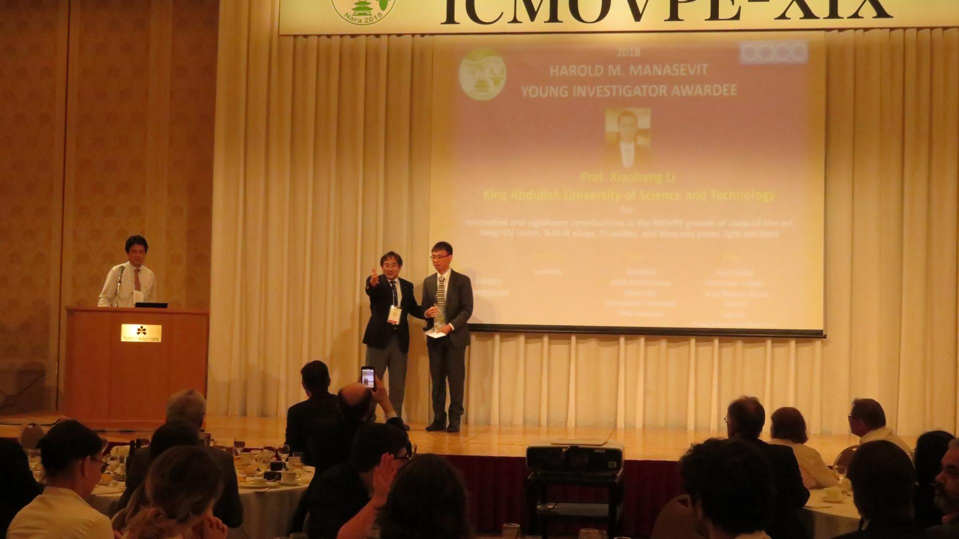
- Harold M. Manasevit Young Investigator Award, American Association of Crystal Growth (AACG), 2018
- Official Nominee of KAUST Distinguished Teaching Award, KAUST, 2018
- Elected Representative in University Academic Counsel, KAUST, 2017-2019
- Title of the Weekly News Letter (1), Compound Semiconductor, 2017
- Title of the Weekly News Letter (2), Compound Semiconductor, 2017
- Editor’s Select, Applied Physics Letter, 2016
- Georgia Tech representative, Global Young Scientist Summit, 2015
- Graduate Student Fellowship, IEEE Photonics Society, 2014
- Steve W. Chaddick Fellowship, Georgia Institute of Technology, 2014
- Anne Robinson Clough International Student Grant, Georgia Institute of Technology, 2014
- D. J. Lovell Scholarship, SPIE, 2013
- Edison Prize, Georgia Institute of Technology, Edison Innovation Foundation, 2013
- Member of Insight Engineering & Science Program, McKinsey & Company, 2013
- Member of Bridge to BCG Program, Boston Consulting Group, 2013
- Most Commercialize Prize, Georgia Institute of Technology, 2013
- Best Product Showcase Prize, Georgia Institute of Technology, 2013
- Innovation Alley, Lehigh Valley, TEDx, 2013
- Immigrant Innovator and Entrepreneur Awarding Ceremony, the U.S. White House, 2013
- Best Customer Discovery Award, Georgia Tech, 2012
- First Place of Elevator Pitch Competition, Georgia Institute of Technology, 2012
- Michael W Levin’87 Advanced Technology Award, Lehigh University, 2012
- National Scholarship, China, 2008