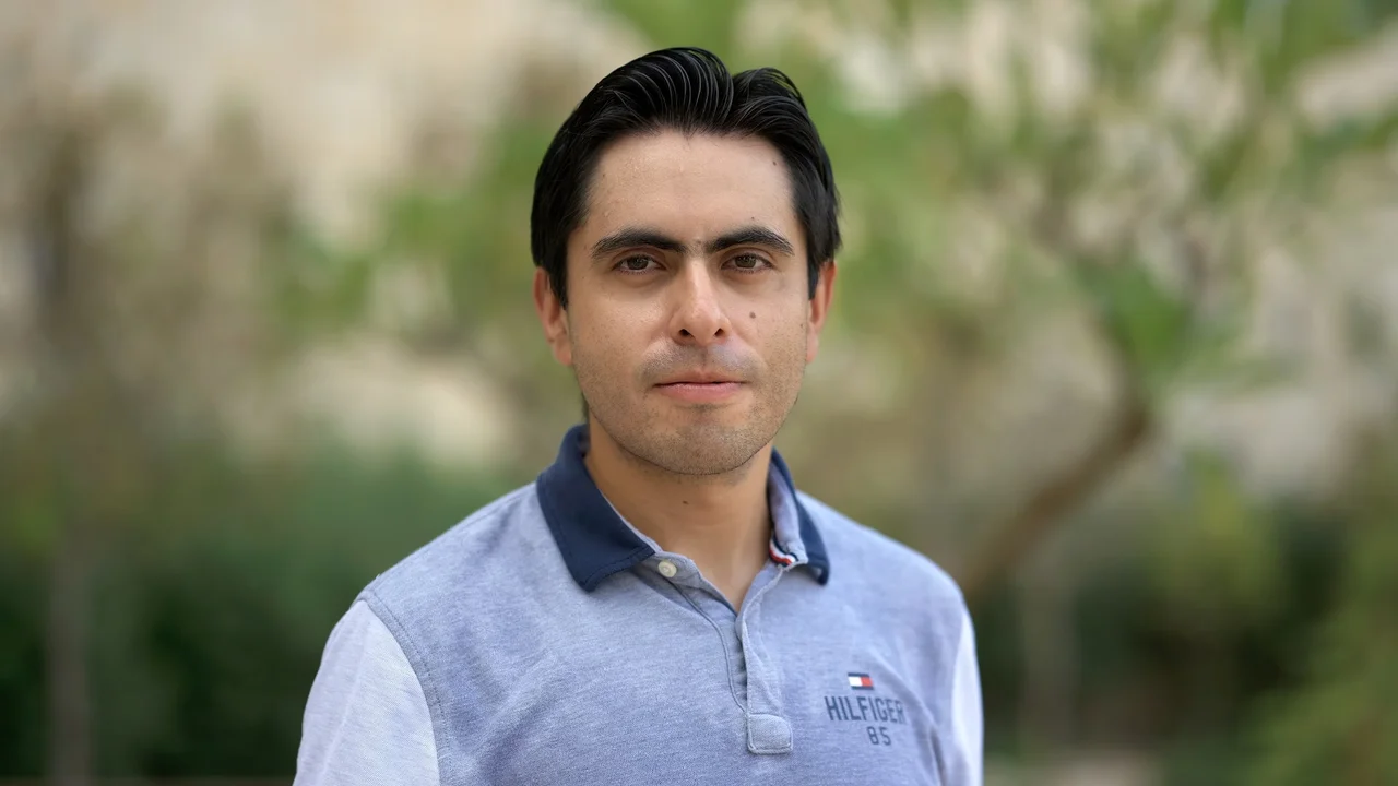
Hanchen Gan
- Ph.D. Student
Biography
Hanchen Gan received the M.S. degree in microelectronics from the Institute of Microelectronics, Chinese Academy of Sciences (IMECAS), Beijing, China, in 2024, where he was affiliated with the National Key Laboratory of Integrated Circuit Manufacturing—3D Integration and System Packaging Laboratory.
From March to October 2024, he worked at Cadence as a Product Validation Engineer. He worked in the CPG Group, validating the Clarity 3D full-wave electromagnetic solver. From November 2024 to August 2025, he was a visiting student with the GBDTC Electromagnetic Informatics Lab at the University of Technology Sydney (UTs).
Expertise and Interests
Hanchen’s research interests span antenna design (antenna-in-package (AiP), mmWave phased arrays, base-station antennas, transmissive metasurface antennas) and semiconductor advanced packaging (2.5D/3D packaging,signal and power integrity, die-to-die (D2D) interconnects for chiplets).